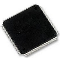
LCMXO2280C-5TN144C LATTICE SEMICONDUCTOR, LCMXO2280C-5TN144C Datasheet - Page 136

LCMXO2280C-5TN144C
Manufacturer Part Number
LCMXO2280C-5TN144C
Description
MACHXO PLD FLASH, SCRAM 1.8V, SMD
Manufacturer
LATTICE SEMICONDUCTOR
Series
MachXOr
Datasheet
1.LCMXO1200C-5TN144C.pdf
(244 pages)
Specifications of LCMXO2280C-5TN144C
Cpld Type
FLASH
No. Of Macrocells
1140
No. Of I/o's
113
Propagation Delay
3.6ns
Global Clock Setup Time
1.1ns
Frequency
600MHz
Supply Voltage Range
1.71V To 3.465V
Operating
RoHS Compliant
Available stocks
Company
Part Number
Manufacturer
Quantity
Price
Company:
Part Number:
LCMXO2280C-5TN144C
Manufacturer:
Lattice Semiconductor Corporation
Quantity:
10 000
Part Number:
LCMXO2280C-5TN144C
Manufacturer:
LATTICE/莱迪斯
Quantity:
20 000
- Current page: 136 of 244
- Download datasheet (9Mb)
Lattice Semiconductor
Table 9-4. EBR based True Dual Port Memory Port Definitions
Reset (or RST) resets only the input and output registers of the RAM. It does not reset the contents of the memory.
Chip Select (CS) is a useful port in the EBR primitive when multiple cascaded EBR blocks are required by the
memory. The CS signal forms the MSB for the address when multiple EBR blocks are cascaded. Since CS is a 3-
bit bus, it can cascade eight memories easily. However, if the memory size specified by the user requires more than
eight EBR blocks, the ispLEVER or Diamond software automatically generates the additional address decoding
logic, which is implemented in the PFU external to the EBR blocks.
Each EBR block consists of 9,216 bits of RAM. The values for x’s (for address) and y’s (data) for each EBR block
for the devices are listed in Table 9-5.
Table 9-5. MachXO Dual Port Memory Sizes for 9K Memory
Table 9-6 shows the various attributes available for the True Dual Port Memory (RAM_DP_TRUE). Some of these
attributes are user-selectable through the IPexpress GUI. For detailed attribute definitions, refer to the Appendix A.
ClockA, ClockB
ClockEnA, ClockEnB
AddressA, AddressB
DataA, DataB
QA, QB
WrA, WrB
ResetA, ResetB
Memory Size
Dual Port
512 x 18
8K x 1
4K x 2
2K x 4
1K x 9
Generated Module
Port Name in
Input Data
DIA[17:0]
DIA[1:0]
DIA[3:0]
DIA[8:0]
Port A
DIA
CLKA, CLKB
CEA, CEB
ADA[x1:0], ADB[x2:0]
DIA[y1:0], DIB[y2:0]
DOA[y1:0], DOB[y2:0]
WEA, WEB
RSTA, RSTB
CSA[2:0], CSB[2:0]
EBR Block Primitive
Port Name in the
Input Data
DIB[17:0]
DIB[1:0]
DIB[3:0]
DIB[8:0]
Port B
DIB
Output Data
DOA[17:0]
DOA[1:0]
DOA[3:0]
DOA[8:0]
Port A
DOA
9-13
Clock for PortA and PortB
Clock Enables for Port CLKA
and CLKB
Address Bus Port A and Port B
Input Data Port A and Port B
Output Data Port A and Port B
Write enable Port A and Port B
Reset for PortA and PortB
Chip Selects for each port
Memory Usage Guide for MachXO Devices
Description
Output Data
DOB[17:0]
DOB[1:0]
DOB[3:0]
DOB[8:0]
Port B
DOB
Address Port A
[MSB:LSB]
ADA[12:0]
ADA[11:0]
ADA[10:0]
ADA[9:0]
ADA[8:0]
Rising Clock Edge
Active State
Active High
Active High
Active High
Address Port B
—
—
—
—
[MSB:LSB]
ADB[12:0]
ADB[11:0]
ADB[10:0]
ADB[9:0]
ADB[8:0]
Related parts for LCMXO2280C-5TN144C
Image
Part Number
Description
Manufacturer
Datasheet
Request
R
Part Number:
Description:
IC, CPLD, FLASH, 2280 MACROCELL FTBGA256
Manufacturer:
LATTICE SEMICONDUCTOR
Part Number:
Description:
CPLD MachXO Family 1140 Macro Cells 1.8V/2.5V/3.3V 324-Pin FTBGA Tray
Manufacturer:
LATTICE SEMICONDUCTOR
Datasheet:

Part Number:
Description:
Microcontroller Modules & Accessories MACHXO CNRL EVB
Manufacturer:
Lattice
Datasheet:

Part Number:
Description:
IC, CPLD, FLASH, 2280 MACROCELL, TQFP144
Manufacturer:
LATTICE SEMICONDUCTOR

Part Number:
Description:
MACHXO PLD FLASH, SCRAM 1.8V, SMD
Manufacturer:
LATTICE SEMICONDUCTOR
Datasheet:
Part Number:
Description:
CPLD MachXO Family 1140 Macro Cells 1.8V/2.5V/3.3V 256-Pin FTBGA Tray
Manufacturer:
LATTICE SEMICONDUCTOR
Datasheet:
Part Number:
Description:
CPLD MachXO Family 1140 Macro Cells 1.8V/2.5V/3.3V 324-Pin FTBGA Tray
Manufacturer:
LATTICE SEMICONDUCTOR
Datasheet:
Part Number:
Description:
CPLD MachXO Family 1140 Macro Cells 1.8V/2.5V/3.3V 100-Pin TQFP Tray
Manufacturer:
LATTICE SEMICONDUCTOR
Datasheet:
Part Number:
Description:
ISPLSI2032-80LT44Lattice Semiconductor [In-System Programmable High Density PLD]
Manufacturer:
Lattice Semiconductor Corp.
Datasheet:
Part Number:
Description:
IC PROGRAMMED LATTICE GAL 16V8
Manufacturer:
Lattice Semiconductor Corp.
Datasheet:
Part Number:
Description:
357-036-542-201 CARDEDGE 36POS DL .156 BLK LOPRO
Manufacturer:
Lattice Semiconductor Corp.
Datasheet:
Part Number:
Description:
357-036-542-201 CARDEDGE 36POS DL .156 BLK LOPRO
Manufacturer:
Lattice Semiconductor Corp.
Datasheet:
Part Number:
Description:
357-036-542-201 CARDEDGE 36POS DL .156 BLK LOPRO
Manufacturer:
Lattice Semiconductor Corp.
Datasheet:
Part Number:
Description:
357-036-542-201 CARDEDGE 36POS DL .156 BLK LOPRO
Manufacturer:
Lattice Semiconductor Corp.
Datasheet:


