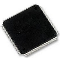
LCMXO2280C-5TN144C LATTICE SEMICONDUCTOR, LCMXO2280C-5TN144C Datasheet - Page 219

LCMXO2280C-5TN144C
Manufacturer Part Number
LCMXO2280C-5TN144C
Description
MACHXO PLD FLASH, SCRAM 1.8V, SMD
Manufacturer
LATTICE SEMICONDUCTOR
Series
MachXOr
Datasheet
1.LCMXO1200C-5TN144C.pdf
(244 pages)
Specifications of LCMXO2280C-5TN144C
Cpld Type
FLASH
No. Of Macrocells
1140
No. Of I/o's
113
Propagation Delay
3.6ns
Global Clock Setup Time
1.1ns
Frequency
600MHz
Supply Voltage Range
1.71V To 3.465V
Operating
RoHS Compliant
Available stocks
Company
Part Number
Manufacturer
Quantity
Price
Company:
Part Number:
LCMXO2280C-5TN144C
Manufacturer:
Lattice Semiconductor Corporation
Quantity:
10 000
Part Number:
LCMXO2280C-5TN144C
Manufacturer:
LATTICE/莱迪斯
Quantity:
20 000
- Current page: 219 of 244
- Download datasheet (9Mb)
Lattice Semiconductor
The following are guidelines for coding the Clock Enable in Lattice Semiconductor FPGAs:
SET / Reset
There are two types of set/reset functions in Lattice Semiconductor FPGAs: Global (GSR) and Local (LSR). The
GSR signal is asynchronous and is used to initialize all registers during configuration. It can be activated either by
an external dedicated pin or from internal logic after configuration. The local SET/Reset signal may be synchro-
nous or asynchronous. GSR is pulsed at power up to either set or reset the registers depending on the configura-
tion of the device. Since the GSR signal has dedicated routing resources that connect to the set and reset pin of
the flip-flops, it saves general-purpose routing and buffering resources and improves overall performance. If asyn-
chronous reset is used in the design, it is recommended to use the GSR for this function, if possible. The reset sig-
nal can be forced to be GSR by the instantiation library element. Synthesis tools will automatically infer GSR if all
• Clock Enable is only supported by FFs, not latches.
• Nibble wide FFs and slices inside a PFU share the same Clock Enable
• All flip-flops in the Lattice Semiconductor FPGA library have a positive clock enable signal
• In the ORCA Series 4 architecture, the Clock Enable signal has the higher priority over synchronous
set/reset by default. However, it can be programmed to have the priority of synchronous LSR over the prior-
ity of Clock Enable. This can be achieved by instantiating the library element in the source code. For exam-
ple, the library element FD1P3IX is a flip-flop that allows synchronous Clear to override Clock Enable.
Users can also specify the priority of generic coding by setting the priority of the control signals differently.
The following examples demonstrate coding methodologies to help the synthesis tools to set the higher pri-
ority of Clock Enable or synchronous LSR.
-- VHDL Example of CE over Sync. LSR
...
COUNT8: process(CLK, GRST)
begin
end process COUNT8;
-- VHDL Example of Sync. LSR Over CE
...
COUNT8: process(CLK, GRST)
begin
if (GRST = '1') then
elsif (CLK'event and CLK='1') then
-- CE Over LSR: Clock Enable has higher priority
end if;
if (GRST = '1') then
elsif (CLK'event and CLK='1') then
-- LSR over CE: Sync. Set/Reset has higher priority
cnt <= (others => '0');
if (CKEN = '1') then
elsif (LRST = '1') then
end if;
cnt <= (others => '0');
if (LRST = '1') then
elsif (CKEN = '1') then
end if;
cnt <= (others => '0');
cnt <= cnt + 1;
cnt <= cnt + 1;
cnt <= (others =>'0');
13-13
// Verilog Example of CE over Sync. LSR
...
always @(posedge CLK or posedge GRST)
begin
end...
// Verilog Example of Sync. LSR Over CE
...
always @(posedge CLK or posedge GRST)
begin
end
...
if (GRST)
else
if (GRST)
else if (LRST)
else if (CKEN)
cnt = 4'b0;
if (CKEN)
else if (LRST)
cnt = 4'b0;
cnt = 4'b0;
cnt = cnt + 1'b1;
HDL Synthesis Coding Guidelines
cnt = cnt + 1'b1;
cnt = 4'b0;
for Lattice Semiconductor FPGAs
Related parts for LCMXO2280C-5TN144C
Image
Part Number
Description
Manufacturer
Datasheet
Request
R
Part Number:
Description:
IC, CPLD, FLASH, 2280 MACROCELL FTBGA256
Manufacturer:
LATTICE SEMICONDUCTOR
Part Number:
Description:
CPLD MachXO Family 1140 Macro Cells 1.8V/2.5V/3.3V 324-Pin FTBGA Tray
Manufacturer:
LATTICE SEMICONDUCTOR
Datasheet:

Part Number:
Description:
Microcontroller Modules & Accessories MACHXO CNRL EVB
Manufacturer:
Lattice
Datasheet:

Part Number:
Description:
IC, CPLD, FLASH, 2280 MACROCELL, TQFP144
Manufacturer:
LATTICE SEMICONDUCTOR

Part Number:
Description:
MACHXO PLD FLASH, SCRAM 1.8V, SMD
Manufacturer:
LATTICE SEMICONDUCTOR
Datasheet:
Part Number:
Description:
CPLD MachXO Family 1140 Macro Cells 1.8V/2.5V/3.3V 256-Pin FTBGA Tray
Manufacturer:
LATTICE SEMICONDUCTOR
Datasheet:
Part Number:
Description:
CPLD MachXO Family 1140 Macro Cells 1.8V/2.5V/3.3V 324-Pin FTBGA Tray
Manufacturer:
LATTICE SEMICONDUCTOR
Datasheet:
Part Number:
Description:
CPLD MachXO Family 1140 Macro Cells 1.8V/2.5V/3.3V 100-Pin TQFP Tray
Manufacturer:
LATTICE SEMICONDUCTOR
Datasheet:
Part Number:
Description:
ISPLSI2032-80LT44Lattice Semiconductor [In-System Programmable High Density PLD]
Manufacturer:
Lattice Semiconductor Corp.
Datasheet:
Part Number:
Description:
IC PROGRAMMED LATTICE GAL 16V8
Manufacturer:
Lattice Semiconductor Corp.
Datasheet:
Part Number:
Description:
357-036-542-201 CARDEDGE 36POS DL .156 BLK LOPRO
Manufacturer:
Lattice Semiconductor Corp.
Datasheet:
Part Number:
Description:
357-036-542-201 CARDEDGE 36POS DL .156 BLK LOPRO
Manufacturer:
Lattice Semiconductor Corp.
Datasheet:
Part Number:
Description:
357-036-542-201 CARDEDGE 36POS DL .156 BLK LOPRO
Manufacturer:
Lattice Semiconductor Corp.
Datasheet:
Part Number:
Description:
357-036-542-201 CARDEDGE 36POS DL .156 BLK LOPRO
Manufacturer:
Lattice Semiconductor Corp.
Datasheet:


