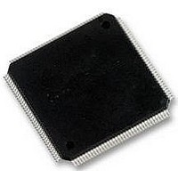
LCMXO2280C-5TN144C LATTICE SEMICONDUCTOR, LCMXO2280C-5TN144C Datasheet - Page 237

LCMXO2280C-5TN144C
Manufacturer Part Number
LCMXO2280C-5TN144C
Description
MACHXO PLD FLASH, SCRAM 1.8V, SMD
Manufacturer
LATTICE SEMICONDUCTOR
Series
MachXOr
Datasheet
1.LCMXO1200C-5TN144C.pdf
(244 pages)
Specifications of LCMXO2280C-5TN144C
Cpld Type
FLASH
No. Of Macrocells
1140
No. Of I/o's
113
Propagation Delay
3.6ns
Global Clock Setup Time
1.1ns
Frequency
600MHz
Supply Voltage Range
1.71V To 3.465V
Operating
RoHS Compliant
Available stocks
Company
Part Number
Manufacturer
Quantity
Price
Company:
Part Number:
LCMXO2280C-5TN144C
Manufacturer:
Lattice Semiconductor Corporation
Quantity:
10 000
Part Number:
LCMXO2280C-5TN144C
Manufacturer:
LATTICE/莱迪斯
Quantity:
20 000
- Current page: 237 of 244
- Download datasheet (9Mb)
PCB Layout Recommendations
Lattice Semiconductor
for BGA Packages
Stack-up types, ordered by cost, high-to-low include:
• High-Density Interconnect (HDI) build up with micro vias
• Laminated with blind and buried vias
• Laminated with through vias
Figure 14-12. Stack-up Example
HDI is a “sandwich” with older-style larger geometry in the middle with fully drilled through holes and then a stack
of fine geometry of blind, buried or mixed via, laminated both on the top and bottom of the middle stack-up. The
laminated layers are thinner than traditional layers and allow finer drilling technology. Staggered micro vias allow
vias within close tolerance or connected to a BGA pad to go down to the next layer or more to route away for
escape routing or underneath the BGA device for further interconnect. HDI type interconnect is used on complex
boards and takes extra steps in the processing flow due to special drilling, plating an laminations. It is a mix of older
technology mixed with newer technology that results in a board that is highly routable.
Figure 14-13. HDI Stack-up with Staggered Micro Vias
Advantages and Disadvantages of BGA Packaging
As pin counts increase and board space becomes more valuable, it is important to place as many circuits per
square inch as possible. BGA offer the best I/O density for a given PCB area. Lattice offers a range of packages
from a 4x4 mm 64-ball csBGA to a 33x33 mm 1704-ball fcBGA.
One of the greatest advantages of BGA packaging is that it can be supported with existing placement and assem-
bly equipment. BGAs also offer significantly more misalignment tolerance and less susceptibility to co-planarity
issues. Even if the solder paste is misaligned or the device is slightly offset, the BGA will self-center during the
14-14
Related parts for LCMXO2280C-5TN144C
Image
Part Number
Description
Manufacturer
Datasheet
Request
R
Part Number:
Description:
IC, CPLD, FLASH, 2280 MACROCELL FTBGA256
Manufacturer:
LATTICE SEMICONDUCTOR
Part Number:
Description:
CPLD MachXO Family 1140 Macro Cells 1.8V/2.5V/3.3V 324-Pin FTBGA Tray
Manufacturer:
LATTICE SEMICONDUCTOR
Datasheet:

Part Number:
Description:
Microcontroller Modules & Accessories MACHXO CNRL EVB
Manufacturer:
Lattice
Datasheet:

Part Number:
Description:
IC, CPLD, FLASH, 2280 MACROCELL, TQFP144
Manufacturer:
LATTICE SEMICONDUCTOR

Part Number:
Description:
MACHXO PLD FLASH, SCRAM 1.8V, SMD
Manufacturer:
LATTICE SEMICONDUCTOR
Datasheet:
Part Number:
Description:
CPLD MachXO Family 1140 Macro Cells 1.8V/2.5V/3.3V 256-Pin FTBGA Tray
Manufacturer:
LATTICE SEMICONDUCTOR
Datasheet:
Part Number:
Description:
CPLD MachXO Family 1140 Macro Cells 1.8V/2.5V/3.3V 324-Pin FTBGA Tray
Manufacturer:
LATTICE SEMICONDUCTOR
Datasheet:
Part Number:
Description:
CPLD MachXO Family 1140 Macro Cells 1.8V/2.5V/3.3V 100-Pin TQFP Tray
Manufacturer:
LATTICE SEMICONDUCTOR
Datasheet:
Part Number:
Description:
ISPLSI2032-80LT44Lattice Semiconductor [In-System Programmable High Density PLD]
Manufacturer:
Lattice Semiconductor Corp.
Datasheet:
Part Number:
Description:
IC PROGRAMMED LATTICE GAL 16V8
Manufacturer:
Lattice Semiconductor Corp.
Datasheet:
Part Number:
Description:
357-036-542-201 CARDEDGE 36POS DL .156 BLK LOPRO
Manufacturer:
Lattice Semiconductor Corp.
Datasheet:
Part Number:
Description:
357-036-542-201 CARDEDGE 36POS DL .156 BLK LOPRO
Manufacturer:
Lattice Semiconductor Corp.
Datasheet:
Part Number:
Description:
357-036-542-201 CARDEDGE 36POS DL .156 BLK LOPRO
Manufacturer:
Lattice Semiconductor Corp.
Datasheet:
Part Number:
Description:
357-036-542-201 CARDEDGE 36POS DL .156 BLK LOPRO
Manufacturer:
Lattice Semiconductor Corp.
Datasheet:


