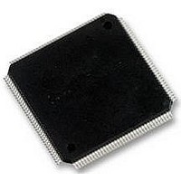
LCMXO2280C-5TN144C LATTICE SEMICONDUCTOR, LCMXO2280C-5TN144C Datasheet - Page 147

LCMXO2280C-5TN144C
Manufacturer Part Number
LCMXO2280C-5TN144C
Description
MACHXO PLD FLASH, SCRAM 1.8V, SMD
Manufacturer
LATTICE SEMICONDUCTOR
Series
MachXOr
Datasheet
1.LCMXO1200C-5TN144C.pdf
(244 pages)
Specifications of LCMXO2280C-5TN144C
Cpld Type
FLASH
No. Of Macrocells
1140
No. Of I/o's
113
Propagation Delay
3.6ns
Global Clock Setup Time
1.1ns
Frequency
600MHz
Supply Voltage Range
1.71V To 3.465V
Operating
RoHS Compliant
Available stocks
Company
Part Number
Manufacturer
Quantity
Price
Company:
Part Number:
LCMXO2280C-5TN144C
Manufacturer:
Lattice Semiconductor Corporation
Quantity:
10 000
Part Number:
LCMXO2280C-5TN144C
Manufacturer:
LATTICE/莱迪斯
Quantity:
20 000
- Current page: 147 of 244
- Download datasheet (9Mb)
Lattice Semiconductor
Figure 9-25. ROM – Read Only Memory Module Generated by IPexpress
The generated module makes use of these EBR blocks or primitives. For the memory sizes smaller than an EBR
block, the module will be created in one EBR block. If the specified memory is larger than one EBR block, multiple
EBR blocks can be cascaded, in depth or width (as required to create these sizes).
In ROM mode, the address for the port is registered at the input of the memory array. The output data of the mem-
ory is optionally registered at the output.
The various ports and their definitions for the ROM are listed in Table 9-10. The table lists the corresponding ports
for the module generated by IPexpress and for the ROM primitive.
Table 9-10. EBR-based ROM Port Definitions
Reset (RST) resets only the input and output registers of the RAM. It does not reset the contents of the memory.
Chip Select (CS) is a useful port when multiple cascaded EBR blocks are required by the memory. The CS signal
forms the MSB for the address when multiple EBR blocks are cascaded. Since CS is a 3-bit bus, it can cascade
eight memories easily. However, if the memory size specified by the user requires more than eight EBR blocks, the
Diamond or ispLEVER software automatically generates the additional address decoding logic, which is imple-
mented in the PFU external to the EBR blocks.
While generating the ROM using IPexpress, the user must provide the initialization file to pre-initialize the contents
of the ROM. These files are the *.mem files and they can be of Binary, Hex or the Addressed Hex formats. The ini-
tialization files are discussed in detail in the Initializing Memory section of this document.
Users have the option of enabling the output registers for Read Only Memory (ROM). Figures 9-26 and 9-27 show
the internal timing waveforms for the Read Only Memory (ROM) with these options.
Generated Module
Port Name in
OutClockEn
OutClock
Address
Reset
—
OutClockEn
EBR Block Primitive
OutClock
Port Name in the
Address
Reset
AD[x:0]
CS[2:0]
CLK
RST
CE
EBR-based Read Only
9-24
Memory
Memory Usage Guide for MachXO Devices
ROM
Read Address
Clock Enable
Description
Chip Select
Reset
Clock
Q
Rising Clock Edge
Active State
Active High
Active High
—
—
Related parts for LCMXO2280C-5TN144C
Image
Part Number
Description
Manufacturer
Datasheet
Request
R
Part Number:
Description:
IC, CPLD, FLASH, 2280 MACROCELL FTBGA256
Manufacturer:
LATTICE SEMICONDUCTOR
Part Number:
Description:
CPLD MachXO Family 1140 Macro Cells 1.8V/2.5V/3.3V 324-Pin FTBGA Tray
Manufacturer:
LATTICE SEMICONDUCTOR
Datasheet:

Part Number:
Description:
Microcontroller Modules & Accessories MACHXO CNRL EVB
Manufacturer:
Lattice
Datasheet:

Part Number:
Description:
IC, CPLD, FLASH, 2280 MACROCELL, TQFP144
Manufacturer:
LATTICE SEMICONDUCTOR

Part Number:
Description:
MACHXO PLD FLASH, SCRAM 1.8V, SMD
Manufacturer:
LATTICE SEMICONDUCTOR
Datasheet:
Part Number:
Description:
CPLD MachXO Family 1140 Macro Cells 1.8V/2.5V/3.3V 256-Pin FTBGA Tray
Manufacturer:
LATTICE SEMICONDUCTOR
Datasheet:
Part Number:
Description:
CPLD MachXO Family 1140 Macro Cells 1.8V/2.5V/3.3V 324-Pin FTBGA Tray
Manufacturer:
LATTICE SEMICONDUCTOR
Datasheet:
Part Number:
Description:
CPLD MachXO Family 1140 Macro Cells 1.8V/2.5V/3.3V 100-Pin TQFP Tray
Manufacturer:
LATTICE SEMICONDUCTOR
Datasheet:
Part Number:
Description:
ISPLSI2032-80LT44Lattice Semiconductor [In-System Programmable High Density PLD]
Manufacturer:
Lattice Semiconductor Corp.
Datasheet:
Part Number:
Description:
IC PROGRAMMED LATTICE GAL 16V8
Manufacturer:
Lattice Semiconductor Corp.
Datasheet:
Part Number:
Description:
357-036-542-201 CARDEDGE 36POS DL .156 BLK LOPRO
Manufacturer:
Lattice Semiconductor Corp.
Datasheet:
Part Number:
Description:
357-036-542-201 CARDEDGE 36POS DL .156 BLK LOPRO
Manufacturer:
Lattice Semiconductor Corp.
Datasheet:
Part Number:
Description:
357-036-542-201 CARDEDGE 36POS DL .156 BLK LOPRO
Manufacturer:
Lattice Semiconductor Corp.
Datasheet:
Part Number:
Description:
357-036-542-201 CARDEDGE 36POS DL .156 BLK LOPRO
Manufacturer:
Lattice Semiconductor Corp.
Datasheet:


