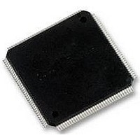
LCMXO2280C-5TN144C LATTICE SEMICONDUCTOR, LCMXO2280C-5TN144C Datasheet - Page 225

LCMXO2280C-5TN144C
Manufacturer Part Number
LCMXO2280C-5TN144C
Description
MACHXO PLD FLASH, SCRAM 1.8V, SMD
Manufacturer
LATTICE SEMICONDUCTOR
Series
MachXOr
Datasheet
1.LCMXO1200C-5TN144C.pdf
(244 pages)
Specifications of LCMXO2280C-5TN144C
Cpld Type
FLASH
No. Of Macrocells
1140
No. Of I/o's
113
Propagation Delay
3.6ns
Global Clock Setup Time
1.1ns
Frequency
600MHz
Supply Voltage Range
1.71V To 3.465V
Operating
RoHS Compliant
Available stocks
Company
Part Number
Manufacturer
Quantity
Price
Company:
Part Number:
LCMXO2280C-5TN144C
Manufacturer:
Lattice Semiconductor Corporation
Quantity:
10 000
Part Number:
LCMXO2280C-5TN144C
Manufacturer:
LATTICE/莱迪斯
Quantity:
20 000
- Current page: 225 of 244
- Download datasheet (9Mb)
Lattice Semiconductor
Table 14-2. Lattice Semiconductor BGA Package Types
BGA Breakout and Routing Examples
Lattice provides several resources and different design implementations that show BGA breakout and routing of
various fine-pitch BGA packages. Different stack up and layer counts are also used to show a range of design rules
and fabrication costs. It is important to consult with your board fabrication and assembly houses as to the most
economical and reliable process for your application.
Currently there is a wide choice of BGAs from Lattice, with many devices offered in multiple packages and pitches
of BGA densities as well as non-BGA options such as TQFP, QFN and others. The BGA pitch or “center to center”
ball dimensions include, 1.00 mm BGAs, space-saving 0.5 mm pitch chip scale BGA and 0.4mm pitch ultra chip
scale BGA packages. Fine pitch packages offer advantages and disadvantages alike. Finer pitch means that the
trace and space limits will have to be adjusted down to match the BGA. Many times a design can get away with
small traces underneath the BGA then fan out with a slightly larger trace width. The PCB fabrication facility will
need to be aware of your design objectives and check for the smallest trace dimensions supported. Smaller traces
take more time to inspect, check and align etc. Etching needs to be closely monitored when trace and space rules
reach their lower limit.
The combination of fanout traces, escape vias, and escape traces that allow routing out from under the BGA pin
array to the perimeter of the device are collectively referred to as the “BGA breakout”. The fanout pattern will
arrange the breakout via, layer, and stack-up to maximize the number of I/Os that can be routed. Fanout patterns
are an important consideration for devices over 800 pins and can be follow polar (north/south/east/west) or layer-
biased directions. (Source: BGA Breakouts and Routing, Charles Pfeil, Mentor Graphics).
Package Type
fpSBGA
caBGA
csBGA
ucBGA
fpBGA
fcBGA
PBGA
ftBGA
SBGA
Plastic BGA with 1.27 mm solder ball pitch. Die up configuration.
Fine Pitch BGA – Plastic BGA with 1.0 mm solder ball pitch. Die up configuration.
Fine Pitch Thin BGA – Thin plastic BGA with 1.0 mm solder ball pitch. Die up configuration.
Chip Array BGA – Plastic BGA with 0.8 mm solder ball pitch. Die up configuration.
Chip Scale BGA – Plastic BGA with 0.5 mm solder ball pitch. Die up configuration.
Flip-Chip BGA with 1.0 mm solder ball pitch. Die down configuration. May have a ceramic or plastic sub-
strate.
Super BGA – Similar to PBGA, but with an integrated heatsink plate. This package has 1.27 mm solder ball
pitch and die down configuration. SBGA packages offer enhanced thermal dissipation capability.
Fine Pitch SBGA – Super BGA with 1.0 mm solder ball pitch. Die down configuration.
Ultra Chip BGA – Saw singulated plastic ball grid array package with 0.4 mm ball pitch.
14-2
Description
PCB Layout Recommendations
for BGA Packages
Related parts for LCMXO2280C-5TN144C
Image
Part Number
Description
Manufacturer
Datasheet
Request
R
Part Number:
Description:
IC, CPLD, FLASH, 2280 MACROCELL FTBGA256
Manufacturer:
LATTICE SEMICONDUCTOR
Part Number:
Description:
CPLD MachXO Family 1140 Macro Cells 1.8V/2.5V/3.3V 324-Pin FTBGA Tray
Manufacturer:
LATTICE SEMICONDUCTOR
Datasheet:

Part Number:
Description:
Microcontroller Modules & Accessories MACHXO CNRL EVB
Manufacturer:
Lattice
Datasheet:

Part Number:
Description:
IC, CPLD, FLASH, 2280 MACROCELL, TQFP144
Manufacturer:
LATTICE SEMICONDUCTOR

Part Number:
Description:
MACHXO PLD FLASH, SCRAM 1.8V, SMD
Manufacturer:
LATTICE SEMICONDUCTOR
Datasheet:
Part Number:
Description:
CPLD MachXO Family 1140 Macro Cells 1.8V/2.5V/3.3V 256-Pin FTBGA Tray
Manufacturer:
LATTICE SEMICONDUCTOR
Datasheet:
Part Number:
Description:
CPLD MachXO Family 1140 Macro Cells 1.8V/2.5V/3.3V 324-Pin FTBGA Tray
Manufacturer:
LATTICE SEMICONDUCTOR
Datasheet:
Part Number:
Description:
CPLD MachXO Family 1140 Macro Cells 1.8V/2.5V/3.3V 100-Pin TQFP Tray
Manufacturer:
LATTICE SEMICONDUCTOR
Datasheet:
Part Number:
Description:
ISPLSI2032-80LT44Lattice Semiconductor [In-System Programmable High Density PLD]
Manufacturer:
Lattice Semiconductor Corp.
Datasheet:
Part Number:
Description:
IC PROGRAMMED LATTICE GAL 16V8
Manufacturer:
Lattice Semiconductor Corp.
Datasheet:
Part Number:
Description:
357-036-542-201 CARDEDGE 36POS DL .156 BLK LOPRO
Manufacturer:
Lattice Semiconductor Corp.
Datasheet:
Part Number:
Description:
357-036-542-201 CARDEDGE 36POS DL .156 BLK LOPRO
Manufacturer:
Lattice Semiconductor Corp.
Datasheet:
Part Number:
Description:
357-036-542-201 CARDEDGE 36POS DL .156 BLK LOPRO
Manufacturer:
Lattice Semiconductor Corp.
Datasheet:
Part Number:
Description:
357-036-542-201 CARDEDGE 36POS DL .156 BLK LOPRO
Manufacturer:
Lattice Semiconductor Corp.
Datasheet:


