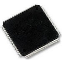
LCMXO2280C-5TN144C LATTICE SEMICONDUCTOR, LCMXO2280C-5TN144C Datasheet - Page 202

LCMXO2280C-5TN144C
Manufacturer Part Number
LCMXO2280C-5TN144C
Description
MACHXO PLD FLASH, SCRAM 1.8V, SMD
Manufacturer
LATTICE SEMICONDUCTOR
Series
MachXOr
Datasheet
1.LCMXO1200C-5TN144C.pdf
(244 pages)
Specifications of LCMXO2280C-5TN144C
Cpld Type
FLASH
No. Of Macrocells
1140
No. Of I/o's
113
Propagation Delay
3.6ns
Global Clock Setup Time
1.1ns
Frequency
600MHz
Supply Voltage Range
1.71V To 3.465V
Operating
RoHS Compliant
Available stocks
Company
Part Number
Manufacturer
Quantity
Price
Company:
Part Number:
LCMXO2280C-5TN144C
Manufacturer:
Lattice Semiconductor Corporation
Quantity:
10 000
Part Number:
LCMXO2280C-5TN144C
Manufacturer:
LATTICE/莱迪斯
Quantity:
20 000
- Current page: 202 of 244
- Download datasheet (9Mb)
MachXO JTAG Programming and
Configuration User’s Guide
June 2010
Technical Note TN1086
Introduction
The MachXO™ is a reconfigurable programmable logic device. The MachXO uses SRAM memory cells to allow
configuring the device to any required functionality. The MachXO also provides non-volatile Flash memory cells to
store the configuration data. The data retrieved from the Flash memory rapidly loads the SRAM memory at power-
up or at the request of the user. This combination of memory types provides several unique programming and oper-
ational capabilities not found in antifuse or SRAM-only based FPGA devices. Some of the capabilities provided by
the MachXO:
• “Instant-on” SRAM loading at power-up
• Bitstream security. Since there is no external PROM there is no access to the bitstream used to program the
MachXO device.
• “Instant” reconfiguration to a known good state from the Flash memory, i.e. recovery from “soft upset events”
• Reprogramming of the Flash while in normal SRAM operation
This technical note describes how to take advantage of these unique capabilities.
Programming Overview
The MachXO contains two types of memory, SRAM and Flash (refer to Figure 12-1). SRAM contains the active
configuration, essentially the “fuses” that define the circuit connections; Flash provides an internal storage space
for the configuration data.
The SRAM can be configured in two ways; by using IEEE 1532 mode via the IEEE 1149.1 compliant ispJTAG™
port or from data stored in the on-chip Flash memory. While writing SRAM via the ispJTAG port the state of the
FPGA’s I/Os is determined by the BSCAN registers. The state of each BSCAN (boundary scan) register can be
determined by the user; available options are high, low, tristate (default), or current value (also called leave alone).
The SRAM may be read without disturbing the operation of the device. This is called transparent, or background
readback. Care must be exercised when reading EBR or distributed RAM, as it is possible to cause conflicts with
accesses from the user design, causing possible data corruption. It is recommended that read/write enables to the
EBR or distributed RAM be turned off any time these resources are being read via the JTAG port.
The on-chip Flash can also be programmed using IEEE 1532 mode via the IEEE 1149.1 compliant ispJTAG port. If
the SRAM portion of the device is blank then the Flash will be programmed using direct mode. In direct mode the
state of the device’s I/Os is determined by the BSCAN registers. The state of each BSCAN register can be deter-
mined by the user; available options are high, low, tristate (default), or current value. If the SRAM portion of the
device is not blank then the Flash will be programmed in background (transparent) mode.
Both SRAM and Flash memory in the MachXO have multiple security fuses to prevent unauthorized readback of
the configuration data. Once set, the only way to clear these security bits is to erase the memory space. A secured
device will read out all zeros.
Note that very early production releases of the MachXO1200 and MachXO2280 marked with a “4W” in the part
number field did not support writes to, or reads from, the SRAM fabric using JTAG. These parts do, however, sup-
port all other programming modes.
© 2010 Lattice Semiconductor Corp. All Lattice trademarks, registered trademarks, patents, and disclaimers are as listed at www.latticesemi.com/legal. All other brand
or product names are trademarks or registered trademarks of their respective holders. The specifications and information herein are subject to change without notice.
www.latticesemi.com
12-1
tn1086_01.4
Related parts for LCMXO2280C-5TN144C
Image
Part Number
Description
Manufacturer
Datasheet
Request
R
Part Number:
Description:
IC, CPLD, FLASH, 2280 MACROCELL FTBGA256
Manufacturer:
LATTICE SEMICONDUCTOR
Part Number:
Description:
CPLD MachXO Family 1140 Macro Cells 1.8V/2.5V/3.3V 324-Pin FTBGA Tray
Manufacturer:
LATTICE SEMICONDUCTOR
Datasheet:

Part Number:
Description:
Microcontroller Modules & Accessories MACHXO CNRL EVB
Manufacturer:
Lattice
Datasheet:

Part Number:
Description:
IC, CPLD, FLASH, 2280 MACROCELL, TQFP144
Manufacturer:
LATTICE SEMICONDUCTOR

Part Number:
Description:
MACHXO PLD FLASH, SCRAM 1.8V, SMD
Manufacturer:
LATTICE SEMICONDUCTOR
Datasheet:
Part Number:
Description:
CPLD MachXO Family 1140 Macro Cells 1.8V/2.5V/3.3V 256-Pin FTBGA Tray
Manufacturer:
LATTICE SEMICONDUCTOR
Datasheet:
Part Number:
Description:
CPLD MachXO Family 1140 Macro Cells 1.8V/2.5V/3.3V 324-Pin FTBGA Tray
Manufacturer:
LATTICE SEMICONDUCTOR
Datasheet:
Part Number:
Description:
CPLD MachXO Family 1140 Macro Cells 1.8V/2.5V/3.3V 100-Pin TQFP Tray
Manufacturer:
LATTICE SEMICONDUCTOR
Datasheet:
Part Number:
Description:
ISPLSI2032-80LT44Lattice Semiconductor [In-System Programmable High Density PLD]
Manufacturer:
Lattice Semiconductor Corp.
Datasheet:
Part Number:
Description:
IC PROGRAMMED LATTICE GAL 16V8
Manufacturer:
Lattice Semiconductor Corp.
Datasheet:
Part Number:
Description:
357-036-542-201 CARDEDGE 36POS DL .156 BLK LOPRO
Manufacturer:
Lattice Semiconductor Corp.
Datasheet:
Part Number:
Description:
357-036-542-201 CARDEDGE 36POS DL .156 BLK LOPRO
Manufacturer:
Lattice Semiconductor Corp.
Datasheet:
Part Number:
Description:
357-036-542-201 CARDEDGE 36POS DL .156 BLK LOPRO
Manufacturer:
Lattice Semiconductor Corp.
Datasheet:
Part Number:
Description:
357-036-542-201 CARDEDGE 36POS DL .156 BLK LOPRO
Manufacturer:
Lattice Semiconductor Corp.
Datasheet:


