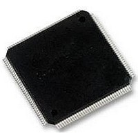
LCMXO2280C-5TN144C LATTICE SEMICONDUCTOR, LCMXO2280C-5TN144C Datasheet - Page 151

LCMXO2280C-5TN144C
Manufacturer Part Number
LCMXO2280C-5TN144C
Description
MACHXO PLD FLASH, SCRAM 1.8V, SMD
Manufacturer
LATTICE SEMICONDUCTOR
Series
MachXOr
Datasheet
1.LCMXO1200C-5TN144C.pdf
(244 pages)
Specifications of LCMXO2280C-5TN144C
Cpld Type
FLASH
No. Of Macrocells
1140
No. Of I/o's
113
Propagation Delay
3.6ns
Global Clock Setup Time
1.1ns
Frequency
600MHz
Supply Voltage Range
1.71V To 3.465V
Operating
RoHS Compliant
Available stocks
Company
Part Number
Manufacturer
Quantity
Price
Company:
Part Number:
LCMXO2280C-5TN144C
Manufacturer:
Lattice Semiconductor Corporation
Quantity:
10 000
Part Number:
LCMXO2280C-5TN144C
Manufacturer:
LATTICE/莱迪斯
Quantity:
20 000
- Current page: 151 of 244
- Download datasheet (9Mb)
Lattice Semiconductor
Similarly, data can be read from the FIFO_DC from the address pointed to by the read counter at the positive edge
of the read clock when read enable is asserted.
Read Pointer Reset (RPReset) is used to indicate a retransmit, and is more commonly used in “packetized” com-
munications. In this application, the user must keep careful track of when a packet is written into or read from the
FIFO_DC.
The data output of the FIFO_DC can be registered or non-registered through a selection in IPexpress. The output
registers are enabled by read enable. A reset will clear the contents of the FIFO_DC by resetting the read and write
pointers and will put the flags in the initial reset state.
FIFO_DC Operation
If the output registers are not enabled it will take two clock cycles to read the first word out. The register for the flag
logic causes this extra clock latency. In the architecture of the emulated FIFO_DC, the internal read enables for
reading the data out is controlled not only by the read enable provided by the user but also the empty flag. When
the data is written into the FIFO, an internal empty flag is registered using write clock that is enabled by write
enable (WrEn). Another clock latency is added due to the clock domain transfer from write clock to read clock using
another register which is clocked by read clock that is enabled by read enable.
Internally, the output of this register is inverted and then ANDed with the user-provided read enable that becomes
the internal read enable to the RAM_DP which is at the core of the FIFO_DC.
Thus, the first read data takes two clock cycles to propagate through. During the first data out, read enable goes
high for one clock cycle, empty flag is de-asserted and is not propagated through the second register enabled by
the read enable. The first clock cycle brings the Empty Low and the second clock cycle brings the internal read
enable high (RdEn and !EF) and then the data is read out by the second clock cycle. Similarly, the first write data
after the full flag has a similar latency.
If the user has enabled the output registers, the output registers will cause an extra clock delay during the first data
out as they are clocked by the read clock and enabled by the read enable.
1. First RdEn and Clock Cycle to propagate the EF internally.
2. Second RdEn and Clock Cycle to generate internal Read Enable into the DPRAM.
3. Third RdEn and Clock Cycle to get the data out of the output registers.
9-28
Memory Usage Guide for MachXO Devices
Related parts for LCMXO2280C-5TN144C
Image
Part Number
Description
Manufacturer
Datasheet
Request
R
Part Number:
Description:
IC, CPLD, FLASH, 2280 MACROCELL FTBGA256
Manufacturer:
LATTICE SEMICONDUCTOR
Part Number:
Description:
CPLD MachXO Family 1140 Macro Cells 1.8V/2.5V/3.3V 324-Pin FTBGA Tray
Manufacturer:
LATTICE SEMICONDUCTOR
Datasheet:

Part Number:
Description:
Microcontroller Modules & Accessories MACHXO CNRL EVB
Manufacturer:
Lattice
Datasheet:

Part Number:
Description:
IC, CPLD, FLASH, 2280 MACROCELL, TQFP144
Manufacturer:
LATTICE SEMICONDUCTOR

Part Number:
Description:
MACHXO PLD FLASH, SCRAM 1.8V, SMD
Manufacturer:
LATTICE SEMICONDUCTOR
Datasheet:
Part Number:
Description:
CPLD MachXO Family 1140 Macro Cells 1.8V/2.5V/3.3V 256-Pin FTBGA Tray
Manufacturer:
LATTICE SEMICONDUCTOR
Datasheet:
Part Number:
Description:
CPLD MachXO Family 1140 Macro Cells 1.8V/2.5V/3.3V 324-Pin FTBGA Tray
Manufacturer:
LATTICE SEMICONDUCTOR
Datasheet:
Part Number:
Description:
CPLD MachXO Family 1140 Macro Cells 1.8V/2.5V/3.3V 100-Pin TQFP Tray
Manufacturer:
LATTICE SEMICONDUCTOR
Datasheet:
Part Number:
Description:
ISPLSI2032-80LT44Lattice Semiconductor [In-System Programmable High Density PLD]
Manufacturer:
Lattice Semiconductor Corp.
Datasheet:
Part Number:
Description:
IC PROGRAMMED LATTICE GAL 16V8
Manufacturer:
Lattice Semiconductor Corp.
Datasheet:
Part Number:
Description:
357-036-542-201 CARDEDGE 36POS DL .156 BLK LOPRO
Manufacturer:
Lattice Semiconductor Corp.
Datasheet:
Part Number:
Description:
357-036-542-201 CARDEDGE 36POS DL .156 BLK LOPRO
Manufacturer:
Lattice Semiconductor Corp.
Datasheet:
Part Number:
Description:
357-036-542-201 CARDEDGE 36POS DL .156 BLK LOPRO
Manufacturer:
Lattice Semiconductor Corp.
Datasheet:
Part Number:
Description:
357-036-542-201 CARDEDGE 36POS DL .156 BLK LOPRO
Manufacturer:
Lattice Semiconductor Corp.
Datasheet:


