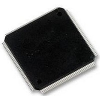
LCMXO2280C-5TN144C LATTICE SEMICONDUCTOR, LCMXO2280C-5TN144C Datasheet - Page 164

LCMXO2280C-5TN144C
Manufacturer Part Number
LCMXO2280C-5TN144C
Description
MACHXO PLD FLASH, SCRAM 1.8V, SMD
Manufacturer
LATTICE SEMICONDUCTOR
Series
MachXOr
Datasheet
1.LCMXO1200C-5TN144C.pdf
(244 pages)
Specifications of LCMXO2280C-5TN144C
Cpld Type
FLASH
No. Of Macrocells
1140
No. Of I/o's
113
Propagation Delay
3.6ns
Global Clock Setup Time
1.1ns
Frequency
600MHz
Supply Voltage Range
1.71V To 3.465V
Operating
RoHS Compliant
Available stocks
Company
Part Number
Manufacturer
Quantity
Price
Company:
Part Number:
LCMXO2280C-5TN144C
Manufacturer:
Lattice Semiconductor Corporation
Quantity:
10 000
Part Number:
LCMXO2280C-5TN144C
Manufacturer:
LATTICE/莱迪斯
Quantity:
20 000
- Current page: 164 of 244
- Download datasheet (9Mb)
Lattice Semiconductor
Figure 10-2. PLL Block Diagram
Features
• Clock synthesis
• Phase shift/duty cycle selection
• Internal, clock tree and external feedback
• Dynamic delay adjustment
• No external components required
• Lock detect output
Functional Description
PLL Divider and Delay Blocks
Input Clock (CLKI) Divider
The CLKI divider is used to control the input clock frequency into the PLL block. The divider setting directly corre-
sponds to the divisor of the output clock. The input and output of the input divider must be within the input and out-
put frequency ranges specified in the
Feedback Loop (CLKFB) Divider
The CLKFB divider is used to divide the feedback signal. Effectively, this multiplies the output clock, because the
divided feedback must speed up to match the input frequency into the PLL block. The PLL block increases the out-
put frequency until the divided feedback frequency equals the input frequency.The input and output of the feedback
divider must be within the input and output frequency ranges specified in the
Delay Adjustment
The delay adjust circuit provides programmable clock delay. The programmable clock delay allows for step delays
in increments of 250ps (nominal) for a total of 2.00ns lagging or leading. The time delay setting has a tolerance.
See the
affected. The delay adjustment has two modes of operation:
Static Delay Adjustment: In this mode, the user-selected delay is configured at power-up.
Dynamic Delay Adjustment (DDA): In this mode, a simple bus is used to configure the delay. The bus signals are
available to the general purpose FPGA.
Output Clock (CLKOP) Divider
The CLKOP divider serves the dual purposes of squaring the duty cycle of the VCO output and scaling up the VCO
frequency into the 420MHz to 840MHz range to minimize jitter. Refer to Table for CLKOP Divider values.
DDAIDEL[2:0]
DDAMODE
DDAILAG
DDAIZR
CLKFB
MachXO Family Data Sheet
CLKI
RST
CLKFB
Divider
Divider
CLKI
MachXO Family Data
for details. Under this mode, CLKOP, CLKOS and CLKOK are identically
Delay
Fine
Frequency
Detector
Phase
&
Clocktree Feedback
10-2
Internal Feedback
Loop
Filter
Sheet.
VCO
Detect
Lock
CLKOP
Divider
MachXO Family Data
Design and Usage Guide
MachXO sysCLOCK PLL
Phase/Duty
CLKOK
Divider
Select
CLKINTFB
CLKOK
CLKOS
CLKOP
LOCK
Sheet.
Clock
Tree
Related parts for LCMXO2280C-5TN144C
Image
Part Number
Description
Manufacturer
Datasheet
Request
R
Part Number:
Description:
IC, CPLD, FLASH, 2280 MACROCELL FTBGA256
Manufacturer:
LATTICE SEMICONDUCTOR
Part Number:
Description:
CPLD MachXO Family 1140 Macro Cells 1.8V/2.5V/3.3V 324-Pin FTBGA Tray
Manufacturer:
LATTICE SEMICONDUCTOR
Datasheet:

Part Number:
Description:
Microcontroller Modules & Accessories MACHXO CNRL EVB
Manufacturer:
Lattice
Datasheet:

Part Number:
Description:
IC, CPLD, FLASH, 2280 MACROCELL, TQFP144
Manufacturer:
LATTICE SEMICONDUCTOR

Part Number:
Description:
MACHXO PLD FLASH, SCRAM 1.8V, SMD
Manufacturer:
LATTICE SEMICONDUCTOR
Datasheet:
Part Number:
Description:
CPLD MachXO Family 1140 Macro Cells 1.8V/2.5V/3.3V 256-Pin FTBGA Tray
Manufacturer:
LATTICE SEMICONDUCTOR
Datasheet:
Part Number:
Description:
CPLD MachXO Family 1140 Macro Cells 1.8V/2.5V/3.3V 324-Pin FTBGA Tray
Manufacturer:
LATTICE SEMICONDUCTOR
Datasheet:
Part Number:
Description:
CPLD MachXO Family 1140 Macro Cells 1.8V/2.5V/3.3V 100-Pin TQFP Tray
Manufacturer:
LATTICE SEMICONDUCTOR
Datasheet:
Part Number:
Description:
ISPLSI2032-80LT44Lattice Semiconductor [In-System Programmable High Density PLD]
Manufacturer:
Lattice Semiconductor Corp.
Datasheet:
Part Number:
Description:
IC PROGRAMMED LATTICE GAL 16V8
Manufacturer:
Lattice Semiconductor Corp.
Datasheet:
Part Number:
Description:
357-036-542-201 CARDEDGE 36POS DL .156 BLK LOPRO
Manufacturer:
Lattice Semiconductor Corp.
Datasheet:
Part Number:
Description:
357-036-542-201 CARDEDGE 36POS DL .156 BLK LOPRO
Manufacturer:
Lattice Semiconductor Corp.
Datasheet:
Part Number:
Description:
357-036-542-201 CARDEDGE 36POS DL .156 BLK LOPRO
Manufacturer:
Lattice Semiconductor Corp.
Datasheet:
Part Number:
Description:
357-036-542-201 CARDEDGE 36POS DL .156 BLK LOPRO
Manufacturer:
Lattice Semiconductor Corp.
Datasheet:


