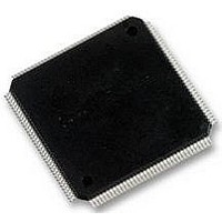
LCMXO2280C-5TN144C LATTICE SEMICONDUCTOR, LCMXO2280C-5TN144C Datasheet - Page 218

LCMXO2280C-5TN144C
Manufacturer Part Number
LCMXO2280C-5TN144C
Description
MACHXO PLD FLASH, SCRAM 1.8V, SMD
Manufacturer
LATTICE SEMICONDUCTOR
Series
MachXOr
Datasheet
1.LCMXO1200C-5TN144C.pdf
(244 pages)
Specifications of LCMXO2280C-5TN144C
Cpld Type
FLASH
No. Of Macrocells
1140
No. Of I/o's
113
Propagation Delay
3.6ns
Global Clock Setup Time
1.1ns
Frequency
600MHz
Supply Voltage Range
1.71V To 3.465V
Operating
RoHS Compliant
Available stocks
Company
Part Number
Manufacturer
Quantity
Price
Company:
Part Number:
LCMXO2280C-5TN144C
Manufacturer:
Lattice Semiconductor Corporation
Quantity:
10 000
Part Number:
LCMXO2280C-5TN144C
Manufacturer:
LATTICE/莱迪斯
Quantity:
20 000
- Current page: 218 of 244
- Download datasheet (9Mb)
Lattice Semiconductor
Register Control Signals
The general-purpose latches/FFs in the PFU are used in a variety of configurations depending on device family. For
example, the Lattice EC, ECP, SC and XP family of devices clock, clock enable and LSR control can be applied to
the registers on a slice basis. Each slice contains two LUT4 lookup tables feeding two registers (programmed asto
be in FF or Latch mode), and some associated logic that allows the LUTs to be combined to perform functions such
as LUT5, LUT6, LUT7 and LUT8. There is control logic to perform set/reset functions (prgorammable as synchro-
nous/asynchronous), clock select, chip-select and wider RAM/ROM functions. The ORCA Series 4 family of
devices clock, clock enable and LSR control can be applied to the registers on a nibble-wide basis. When writing
design codes in HDL, keep the architecture in mind to avoid wasting resources in the device. Here are several
points for consideration:
For more detailed architecture information, refer to the Lattice Semiconductor FPGA data sheets.
Clock Enable
Figure 13-9 shows an example of gated clocking. Gating clock is not encouraged in digital designs because it may
cause timing issues such as unexpected clock skews. The structure of the PFU makes the gating clock even more
undesirable since it will use up all the clock resources in one PFU and sometimes waste the FF/ Latches resources
in the PFU. By using the clock enable in the PFU, the same functionality can be achieved without worrying about
timing issues as only one signal is controlling the clock. Since only one clock is used in the PFU, all related logic
can be implemented in one block to achieve better performance. Figure 13-10 shows the design with clock enable
signal being used.
Figure 13-9. Asynchronous: Gated Clocking
Figure 13-10. Synchronous: Clock Enabling
The VHDL and Verilog coding for Clock Enable are as shown in Figure 13-10.
• If the register number is not a multiple of 2 or 4 (dependent on device family), try to code the registers in a
• Lattice Semiconductor FPGA devices have multiple dedicated Clock Enable signals per PFU. Try to code
• Try to code the registers with Local synchronous Set/Reset and Global asynchronous Set/Reset
way that all registers share the same clock, and in a way that all registers share the same control signals.
the asynchronous clocks as clock enables, so that PFU clock signals can be released to use global low-
skew clocks.
-- VHDL example for Clock Enable
...
Clock_Enable: process(clk)
begin
end process Clock_Enable;
if (clk'event or clk='1') then
end if;
if (clken='1') then
end if;
qout <= din;
clken
gate
din
clk
din
clk
A
B
S
13-12
D
D
// Verilog example for Clock Enable
...
always @(posedge clk)
...
qout <= clken ? din : qout;
Q
Q
HDL Synthesis Coding Guidelines
for Lattice Semiconductor FPGAs
qout
qout
Related parts for LCMXO2280C-5TN144C
Image
Part Number
Description
Manufacturer
Datasheet
Request
R
Part Number:
Description:
IC, CPLD, FLASH, 2280 MACROCELL FTBGA256
Manufacturer:
LATTICE SEMICONDUCTOR
Part Number:
Description:
CPLD MachXO Family 1140 Macro Cells 1.8V/2.5V/3.3V 324-Pin FTBGA Tray
Manufacturer:
LATTICE SEMICONDUCTOR
Datasheet:

Part Number:
Description:
Microcontroller Modules & Accessories MACHXO CNRL EVB
Manufacturer:
Lattice
Datasheet:

Part Number:
Description:
IC, CPLD, FLASH, 2280 MACROCELL, TQFP144
Manufacturer:
LATTICE SEMICONDUCTOR

Part Number:
Description:
MACHXO PLD FLASH, SCRAM 1.8V, SMD
Manufacturer:
LATTICE SEMICONDUCTOR
Datasheet:
Part Number:
Description:
CPLD MachXO Family 1140 Macro Cells 1.8V/2.5V/3.3V 256-Pin FTBGA Tray
Manufacturer:
LATTICE SEMICONDUCTOR
Datasheet:
Part Number:
Description:
CPLD MachXO Family 1140 Macro Cells 1.8V/2.5V/3.3V 324-Pin FTBGA Tray
Manufacturer:
LATTICE SEMICONDUCTOR
Datasheet:
Part Number:
Description:
CPLD MachXO Family 1140 Macro Cells 1.8V/2.5V/3.3V 100-Pin TQFP Tray
Manufacturer:
LATTICE SEMICONDUCTOR
Datasheet:
Part Number:
Description:
ISPLSI2032-80LT44Lattice Semiconductor [In-System Programmable High Density PLD]
Manufacturer:
Lattice Semiconductor Corp.
Datasheet:
Part Number:
Description:
IC PROGRAMMED LATTICE GAL 16V8
Manufacturer:
Lattice Semiconductor Corp.
Datasheet:
Part Number:
Description:
357-036-542-201 CARDEDGE 36POS DL .156 BLK LOPRO
Manufacturer:
Lattice Semiconductor Corp.
Datasheet:
Part Number:
Description:
357-036-542-201 CARDEDGE 36POS DL .156 BLK LOPRO
Manufacturer:
Lattice Semiconductor Corp.
Datasheet:
Part Number:
Description:
357-036-542-201 CARDEDGE 36POS DL .156 BLK LOPRO
Manufacturer:
Lattice Semiconductor Corp.
Datasheet:
Part Number:
Description:
357-036-542-201 CARDEDGE 36POS DL .156 BLK LOPRO
Manufacturer:
Lattice Semiconductor Corp.
Datasheet:


