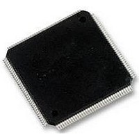
LCMXO2280C-5TN144C LATTICE SEMICONDUCTOR, LCMXO2280C-5TN144C Datasheet - Page 124

LCMXO2280C-5TN144C
Manufacturer Part Number
LCMXO2280C-5TN144C
Description
MACHXO PLD FLASH, SCRAM 1.8V, SMD
Manufacturer
LATTICE SEMICONDUCTOR
Series
MachXOr
Datasheet
1.LCMXO1200C-5TN144C.pdf
(244 pages)
Specifications of LCMXO2280C-5TN144C
Cpld Type
FLASH
No. Of Macrocells
1140
No. Of I/o's
113
Propagation Delay
3.6ns
Global Clock Setup Time
1.1ns
Frequency
600MHz
Supply Voltage Range
1.71V To 3.465V
Operating
RoHS Compliant
Available stocks
Company
Part Number
Manufacturer
Quantity
Price
Company:
Part Number:
LCMXO2280C-5TN144C
Manufacturer:
Lattice Semiconductor Corporation
Quantity:
10 000
Part Number:
LCMXO2280C-5TN144C
Manufacturer:
LATTICE/莱迪斯
Quantity:
20 000
- Current page: 124 of 244
- Download datasheet (9Mb)
October 2010
Introduction
This technical note discusses memory usage for the Lattice MachXO device family. It is intended to be used by
design engineers as a guide in integrating the EBR and PFU based memories for these device families in isp-
LEVER
The architecture of these devices provides resources for memory intensive applications. The sysMEM™ Embed-
ded Block RAM (EBR) complements its distributed PFU-based memory. Single-Port RAM, Dual-Port RAM, Pseudo
Dual-Port RAM, FIFO and ROM memories can be constructed using the EBR. LUTs and PFU can implement Dis-
tributed Single-Port RAM, Dual-Port RAM and ROM.
The capabilities of the EBR Block RAM and PFU RAM are referred to as primitives and are described later in this
document. Designers can utilize the memory primitives in two ways:
• Via IPexpress™ – The IPexpress GUI allows users to specify the memory type and size that is required. IPex-
• Via the PMI (Parameterizable Module Inferencing) – PMI allows experienced users to skip the graphical inter-
The remainder of this document discusses these approaches, utilizing IPexpress, PMI inference, memory modules
and memory primitives.
MachXO Device Memories
Only the MachXO1200 and MachXO2280 devices contain the sysMEM EBR blocks along with an array of logic
blocks called PFUs (or PFFs) surrounded by Programmable I/O Cells (PICs). This is shown in Figure 9-1.
Figure 9-1. Logical View of MachXO1200 and MachXO2280 Devices
© 2010 Lattice Semiconductor Corp. All Lattice trademarks, registered trademarks, patents, and disclaimers are as listed at www.latticesemi.com/legal. All other brand
or product names are trademarks or registered trademarks of their respective holders. The specifications and information herein are subject to change without notice.
www.latticesemi.com
press takes this specification and constructs a netlist to implement the desired memory by using one or more of
the memory primitives.
face and utilize the configurable memory modules on the fly from the ispLEVER Project Navigator or Diamond.
The parameters and the control signals needed either in Verilog or VHDL can be set. The top-level design will
have the parameters defined and signals declared so the interface can automatically generate the black box dur-
ing synthesis.
®
and Lattice Diamond™ design software.
sysMEM Embedded
Block RAM (EBR)
JTAG Port
sysCLOCK PLL
Programmable Functional Unit (PFUs) with RAM
9-1
Memory Usage Guide for
PIOs Arranged into
sysIO Banks
Programmable
Function Units
(PFFs) without
RAM
MachXO Devices
Technical Note TN1092
tn1092_01.5
Related parts for LCMXO2280C-5TN144C
Image
Part Number
Description
Manufacturer
Datasheet
Request
R
Part Number:
Description:
IC, CPLD, FLASH, 2280 MACROCELL FTBGA256
Manufacturer:
LATTICE SEMICONDUCTOR
Part Number:
Description:
CPLD MachXO Family 1140 Macro Cells 1.8V/2.5V/3.3V 324-Pin FTBGA Tray
Manufacturer:
LATTICE SEMICONDUCTOR
Datasheet:

Part Number:
Description:
Microcontroller Modules & Accessories MACHXO CNRL EVB
Manufacturer:
Lattice
Datasheet:

Part Number:
Description:
IC, CPLD, FLASH, 2280 MACROCELL, TQFP144
Manufacturer:
LATTICE SEMICONDUCTOR

Part Number:
Description:
MACHXO PLD FLASH, SCRAM 1.8V, SMD
Manufacturer:
LATTICE SEMICONDUCTOR
Datasheet:
Part Number:
Description:
CPLD MachXO Family 1140 Macro Cells 1.8V/2.5V/3.3V 256-Pin FTBGA Tray
Manufacturer:
LATTICE SEMICONDUCTOR
Datasheet:
Part Number:
Description:
CPLD MachXO Family 1140 Macro Cells 1.8V/2.5V/3.3V 324-Pin FTBGA Tray
Manufacturer:
LATTICE SEMICONDUCTOR
Datasheet:
Part Number:
Description:
CPLD MachXO Family 1140 Macro Cells 1.8V/2.5V/3.3V 100-Pin TQFP Tray
Manufacturer:
LATTICE SEMICONDUCTOR
Datasheet:
Part Number:
Description:
ISPLSI2032-80LT44Lattice Semiconductor [In-System Programmable High Density PLD]
Manufacturer:
Lattice Semiconductor Corp.
Datasheet:
Part Number:
Description:
IC PROGRAMMED LATTICE GAL 16V8
Manufacturer:
Lattice Semiconductor Corp.
Datasheet:
Part Number:
Description:
357-036-542-201 CARDEDGE 36POS DL .156 BLK LOPRO
Manufacturer:
Lattice Semiconductor Corp.
Datasheet:
Part Number:
Description:
357-036-542-201 CARDEDGE 36POS DL .156 BLK LOPRO
Manufacturer:
Lattice Semiconductor Corp.
Datasheet:
Part Number:
Description:
357-036-542-201 CARDEDGE 36POS DL .156 BLK LOPRO
Manufacturer:
Lattice Semiconductor Corp.
Datasheet:
Part Number:
Description:
357-036-542-201 CARDEDGE 36POS DL .156 BLK LOPRO
Manufacturer:
Lattice Semiconductor Corp.
Datasheet:


