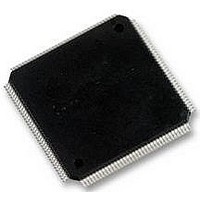
LCMXO2280C-5TN144C LATTICE SEMICONDUCTOR, LCMXO2280C-5TN144C Datasheet - Page 109

LCMXO2280C-5TN144C
Manufacturer Part Number
LCMXO2280C-5TN144C
Description
MACHXO PLD FLASH, SCRAM 1.8V, SMD
Manufacturer
LATTICE SEMICONDUCTOR
Series
MachXOr
Datasheet
1.LCMXO1200C-5TN144C.pdf
(244 pages)
Specifications of LCMXO2280C-5TN144C
Cpld Type
FLASH
No. Of Macrocells
1140
No. Of I/o's
113
Propagation Delay
3.6ns
Global Clock Setup Time
1.1ns
Frequency
600MHz
Supply Voltage Range
1.71V To 3.465V
Operating
RoHS Compliant
Available stocks
Company
Part Number
Manufacturer
Quantity
Price
Company:
Part Number:
LCMXO2280C-5TN144C
Manufacturer:
Lattice Semiconductor Corporation
Quantity:
10 000
Part Number:
LCMXO2280C-5TN144C
Manufacturer:
LATTICE/莱迪斯
Quantity:
20 000
- Current page: 109 of 244
- Download datasheet (9Mb)
Lattice Semiconductor
Programmable Drive
All LVCMOS and LVTTL single-ended drivers have programmable drive strength. This option can be set for each
I/O independently. The table below lists the programmable drive strengths available for each I/O standard. The
actual value will vary with the I/O voltage. The user must consider the maximum allowable current per bank and the
package thermal limit current when selecting the drive strength.
Table 8-5. Programmable Drive Strength
Programmable Slew Rate
Each LVCMOS or LVTTL output buffer pin also has a programmable output slew rate control that can be configured
for either low noise or high-speed performance. Each I/O pin also has an individual slew rate control. This allows a
designer to specify slew rate control on a pin-by-pin basis. This slew rate control affects both the rising edge and
the falling edges.
Open-Drain Control
Each LVCMOS and LVTTL output buffer can be configured to function as an open-drain output. The user can
implement an open-drain output by turning on the OPENDRAIN attribute in the software.
Programmable PCICLAMP
Each sysIO buffer on the top bank of the MachXO1200 and MachXO2280 devices can be configured to support
PCI33. The buffers also have a PCI clamp diode that will be turned on when the sysIO buffer is configured as
PCI33.
The PCI clamp is mainly used when implementing a 3.3V PCI interface. The PCI Specification revision 2.2 requires
the use of clamping diodes for 3.3V operation. For more information on the PCI interface, please refer to the PCI
specification, revision 2.2.
The PCI clamp can also be optionally turned on for LVCMOS and LVTTL sysIO buffers on the top bank of the
MachXO1200 and MachXO2280 devices. In this case, the PCI clamp is used to implement a 5V input interface.
5V Input Interface Using the PCI Clamp Diode
All the I/Os on the top side of the MachXO1200 and MachXO2280 devices (Banks 0 and 1) have a clamp diode
that is used to clamp the voltage at the input to V
to make an input 5V tolerant.
Single-ended I/O Standard
LVCMOS12
LVCMOS15
LVCMOS18
LVCMOS25
LVCMOS33
LVTTL
CCIO
. This clamp diode can be used along with an external resistor
8-6
Programmable Drive (mA)
4, 8, 12, 14
4, 8, 12, 14
4, 8, 12, 14
4, 8, 12, 16
2, 6
4, 8
MachXO sysIO Usage Guide
Related parts for LCMXO2280C-5TN144C
Image
Part Number
Description
Manufacturer
Datasheet
Request
R
Part Number:
Description:
IC, CPLD, FLASH, 2280 MACROCELL FTBGA256
Manufacturer:
LATTICE SEMICONDUCTOR
Part Number:
Description:
CPLD MachXO Family 1140 Macro Cells 1.8V/2.5V/3.3V 324-Pin FTBGA Tray
Manufacturer:
LATTICE SEMICONDUCTOR
Datasheet:

Part Number:
Description:
Microcontroller Modules & Accessories MACHXO CNRL EVB
Manufacturer:
Lattice
Datasheet:

Part Number:
Description:
IC, CPLD, FLASH, 2280 MACROCELL, TQFP144
Manufacturer:
LATTICE SEMICONDUCTOR

Part Number:
Description:
MACHXO PLD FLASH, SCRAM 1.8V, SMD
Manufacturer:
LATTICE SEMICONDUCTOR
Datasheet:
Part Number:
Description:
CPLD MachXO Family 1140 Macro Cells 1.8V/2.5V/3.3V 256-Pin FTBGA Tray
Manufacturer:
LATTICE SEMICONDUCTOR
Datasheet:
Part Number:
Description:
CPLD MachXO Family 1140 Macro Cells 1.8V/2.5V/3.3V 324-Pin FTBGA Tray
Manufacturer:
LATTICE SEMICONDUCTOR
Datasheet:
Part Number:
Description:
CPLD MachXO Family 1140 Macro Cells 1.8V/2.5V/3.3V 100-Pin TQFP Tray
Manufacturer:
LATTICE SEMICONDUCTOR
Datasheet:
Part Number:
Description:
ISPLSI2032-80LT44Lattice Semiconductor [In-System Programmable High Density PLD]
Manufacturer:
Lattice Semiconductor Corp.
Datasheet:
Part Number:
Description:
IC PROGRAMMED LATTICE GAL 16V8
Manufacturer:
Lattice Semiconductor Corp.
Datasheet:
Part Number:
Description:
357-036-542-201 CARDEDGE 36POS DL .156 BLK LOPRO
Manufacturer:
Lattice Semiconductor Corp.
Datasheet:
Part Number:
Description:
357-036-542-201 CARDEDGE 36POS DL .156 BLK LOPRO
Manufacturer:
Lattice Semiconductor Corp.
Datasheet:
Part Number:
Description:
357-036-542-201 CARDEDGE 36POS DL .156 BLK LOPRO
Manufacturer:
Lattice Semiconductor Corp.
Datasheet:
Part Number:
Description:
357-036-542-201 CARDEDGE 36POS DL .156 BLK LOPRO
Manufacturer:
Lattice Semiconductor Corp.
Datasheet:


