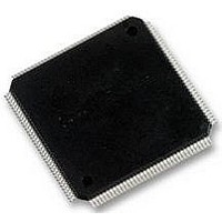
LCMXO2280C-5TN144C LATTICE SEMICONDUCTOR, LCMXO2280C-5TN144C Datasheet - Page 207

LCMXO2280C-5TN144C
Manufacturer Part Number
LCMXO2280C-5TN144C
Description
MACHXO PLD FLASH, SCRAM 1.8V, SMD
Manufacturer
LATTICE SEMICONDUCTOR
Series
MachXOr
Datasheet
1.LCMXO1200C-5TN144C.pdf
(244 pages)
Specifications of LCMXO2280C-5TN144C
Cpld Type
FLASH
No. Of Macrocells
1140
No. Of I/o's
113
Propagation Delay
3.6ns
Global Clock Setup Time
1.1ns
Frequency
600MHz
Supply Voltage Range
1.71V To 3.465V
Operating
RoHS Compliant
Available stocks
Company
Part Number
Manufacturer
Quantity
Price
Company:
Part Number:
LCMXO2280C-5TN144C
Manufacturer:
Lattice Semiconductor Corporation
Quantity:
10 000
Part Number:
LCMXO2280C-5TN144C
Manufacturer:
LATTICE/莱迪斯
Quantity:
20 000
- Current page: 207 of 244
- Download datasheet (9Mb)
October 2005
Introduction
Coding style plays an important role in utilizing FPGA resources. Although many popular synthesis tools have sig-
nificantly improved optimization algorithms for FPGAs, it still is the responsibility of the user to generate meaningful
and efficient HDL code to guide their synthesis tools to achieve the best result for a specific architecture. This appli-
cation note is intended to help designers establish useful HDL coding styles for Lattice Semiconductor FPGA
devices. It includes VHDL and Verilog design guidelines for both novice and experienced users.
The application note is divided into two sections. The general coding styles for FPGAs section provides an over-
view for effective FPGA designs. The following topics are discussed in detail:
The HDL Design with Lattice Semiconductor FPGA Devices section covers specific coding techniques and exam-
ples:
General Coding Styles for FPGA
The following recommendations for common HDL coding styles will help users generate robust and reliable FPGA
designs.
Hierarchical Coding
HDL designs can either be synthesized as a flat module or as many small hierarchical modules. Each methodology
has its advantages and disadvantages. Since designs in smaller blocks are easier to keep track of, it is preferred to
apply hierarchical structure to large and complex FPGA designs. Hierarchical coding methodology allows a group
of engineers to work on one design at the same time. It speeds up design compilation, makes changing the imple-
mentation of key blocks easier, and reduces the design period by allowing the re-use of design modules for current
and future designs. In addition, it produces designs that are easier to understand. However, if the design mapping
into the FPGA is not optimal across hierarchical boundaries, it will lead to lower device utilization and design perfor-
mance. This disadvantage can be overcome with careful design considerations when choosing the design hierar-
chy. Here are some tips for building hierarchical structures:
www.latticesemi.com
• Hierarchical Coding
• Design Partitioning
• Encoding Methodologies for State Machines
• Coding Styles for Finite State Machines (FSM)
• Using Pipelines
• Comparing IF Statements and CASE Statements
• Avoiding Non-intentional Latches
• Using the Lattice Semiconductor FPGA Synthesis Library
• Implementation of Multiplexers
• Creating Clock Dividers
• Register Control Signals (CE, LSR, GSR)
• Using PIC Features
• Implementation of Memories
• Preventing Logic Replication and Fanout
• Comparing Synthesis Results and Place and Route Results
• The top level should only contain instantiation statements to call all major blocks
• Any I/O instantiations should be at the top level
• Any signals going into or out of the devices should be declared as input, output or bi-directional pins at the
top level
HDL Synthesis Coding Guidelines for
Lattice Semiconductor FPGAs
13-1
Technical Note TN1008
tn1008_02.1
Related parts for LCMXO2280C-5TN144C
Image
Part Number
Description
Manufacturer
Datasheet
Request
R
Part Number:
Description:
IC, CPLD, FLASH, 2280 MACROCELL FTBGA256
Manufacturer:
LATTICE SEMICONDUCTOR
Part Number:
Description:
CPLD MachXO Family 1140 Macro Cells 1.8V/2.5V/3.3V 324-Pin FTBGA Tray
Manufacturer:
LATTICE SEMICONDUCTOR
Datasheet:

Part Number:
Description:
Microcontroller Modules & Accessories MACHXO CNRL EVB
Manufacturer:
Lattice
Datasheet:

Part Number:
Description:
IC, CPLD, FLASH, 2280 MACROCELL, TQFP144
Manufacturer:
LATTICE SEMICONDUCTOR

Part Number:
Description:
MACHXO PLD FLASH, SCRAM 1.8V, SMD
Manufacturer:
LATTICE SEMICONDUCTOR
Datasheet:
Part Number:
Description:
CPLD MachXO Family 1140 Macro Cells 1.8V/2.5V/3.3V 256-Pin FTBGA Tray
Manufacturer:
LATTICE SEMICONDUCTOR
Datasheet:
Part Number:
Description:
CPLD MachXO Family 1140 Macro Cells 1.8V/2.5V/3.3V 324-Pin FTBGA Tray
Manufacturer:
LATTICE SEMICONDUCTOR
Datasheet:
Part Number:
Description:
CPLD MachXO Family 1140 Macro Cells 1.8V/2.5V/3.3V 100-Pin TQFP Tray
Manufacturer:
LATTICE SEMICONDUCTOR
Datasheet:
Part Number:
Description:
ISPLSI2032-80LT44Lattice Semiconductor [In-System Programmable High Density PLD]
Manufacturer:
Lattice Semiconductor Corp.
Datasheet:
Part Number:
Description:
IC PROGRAMMED LATTICE GAL 16V8
Manufacturer:
Lattice Semiconductor Corp.
Datasheet:
Part Number:
Description:
357-036-542-201 CARDEDGE 36POS DL .156 BLK LOPRO
Manufacturer:
Lattice Semiconductor Corp.
Datasheet:
Part Number:
Description:
357-036-542-201 CARDEDGE 36POS DL .156 BLK LOPRO
Manufacturer:
Lattice Semiconductor Corp.
Datasheet:
Part Number:
Description:
357-036-542-201 CARDEDGE 36POS DL .156 BLK LOPRO
Manufacturer:
Lattice Semiconductor Corp.
Datasheet:
Part Number:
Description:
357-036-542-201 CARDEDGE 36POS DL .156 BLK LOPRO
Manufacturer:
Lattice Semiconductor Corp.
Datasheet:


