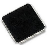
LCMXO2280C-5TN144C LATTICE SEMICONDUCTOR, LCMXO2280C-5TN144C Datasheet - Page 238

LCMXO2280C-5TN144C
Manufacturer Part Number
LCMXO2280C-5TN144C
Description
MACHXO PLD FLASH, SCRAM 1.8V, SMD
Manufacturer
LATTICE SEMICONDUCTOR
Series
MachXOr
Datasheet
1.LCMXO1200C-5TN144C.pdf
(244 pages)
Specifications of LCMXO2280C-5TN144C
Cpld Type
FLASH
No. Of Macrocells
1140
No. Of I/o's
113
Propagation Delay
3.6ns
Global Clock Setup Time
1.1ns
Frequency
600MHz
Supply Voltage Range
1.71V To 3.465V
Operating
RoHS Compliant
Available stocks
Company
Part Number
Manufacturer
Quantity
Price
Company:
Part Number:
LCMXO2280C-5TN144C
Manufacturer:
Lattice Semiconductor Corporation
Quantity:
10 000
Part Number:
LCMXO2280C-5TN144C
Manufacturer:
LATTICE/莱迪斯
Quantity:
20 000
- Current page: 238 of 244
- Download datasheet (9Mb)
PCB Layout Recommendations
Lattice Semiconductor
for BGA Packages
reflow process. This is due to the surface tension of the solder and flux in its molten state pulling each ball into the
center of the pad.
Figure 14-14. Misalignment of BGA Balls vs. QPF Leads
Controlling the oven re-flow profile is one of the most important assembly parameters for consistent and reliable
BGA placement. Profiles are typically tested on a pre-run. One or two panels are run to dial in the process, then
visual and X-ray inspection equipment are used for verification.
BGA packages present numerous benefits previously unobtainable in surface mount packaging technology. BGAs
provide higher pin counts in a much smaller area than was previous possible. No longer is the package design lim-
ited to connections along the periphery on the outside quadrants of the package edge like a PQFP or TQFP out-
line. Fully populated ball grid arrays with pitches as small as 0.4 mm are available.
Some BGA devices are arranged with de-populated interconnect near or around the center. These are dependent
on the die size and number of pins. The area void of interconnect in the middle of the array has some advantages,
it can be used for escape routing vias or tying directly to the ground or power planes.
Although the packages can be quite complex and densely populated, all of these packages receive strict quality
and reliability testing and are widely accepted today by designers and PCB fabrication/assembly houses. All of this
is due to advances in equipment and technology that have allowed a smooth transition into the assembly flow.
BGA Package Test and Assembly
How can a pad/ball/pin be tested that can’t be seen? All connections are hidden under the substrate at the ball
interconnect, making it impossible to directly probe or test. To address this limitation, Lattice programmable devices
provide JTAG, BSCAN, and boundary scan cells that allow electronic test and continuity of each pin with a bound-
ary scan tester. This can be embedded into the system itself or driven externally from a high-speed test head. The
boundary scan can test the pins or board for simple continuity tests or full functional test by shifting in test patterns
through the JTAG port.
For debug or prototype boards it may be necessary to place test points, open vias, or pads to have access to a
given set of pins in order to drive, over-drive or observe a given set of signals. These can be very small, as many
14-15
Related parts for LCMXO2280C-5TN144C
Image
Part Number
Description
Manufacturer
Datasheet
Request
R
Part Number:
Description:
IC, CPLD, FLASH, 2280 MACROCELL FTBGA256
Manufacturer:
LATTICE SEMICONDUCTOR
Part Number:
Description:
CPLD MachXO Family 1140 Macro Cells 1.8V/2.5V/3.3V 324-Pin FTBGA Tray
Manufacturer:
LATTICE SEMICONDUCTOR
Datasheet:

Part Number:
Description:
Microcontroller Modules & Accessories MACHXO CNRL EVB
Manufacturer:
Lattice
Datasheet:

Part Number:
Description:
IC, CPLD, FLASH, 2280 MACROCELL, TQFP144
Manufacturer:
LATTICE SEMICONDUCTOR

Part Number:
Description:
MACHXO PLD FLASH, SCRAM 1.8V, SMD
Manufacturer:
LATTICE SEMICONDUCTOR
Datasheet:
Part Number:
Description:
CPLD MachXO Family 1140 Macro Cells 1.8V/2.5V/3.3V 256-Pin FTBGA Tray
Manufacturer:
LATTICE SEMICONDUCTOR
Datasheet:
Part Number:
Description:
CPLD MachXO Family 1140 Macro Cells 1.8V/2.5V/3.3V 324-Pin FTBGA Tray
Manufacturer:
LATTICE SEMICONDUCTOR
Datasheet:
Part Number:
Description:
CPLD MachXO Family 1140 Macro Cells 1.8V/2.5V/3.3V 100-Pin TQFP Tray
Manufacturer:
LATTICE SEMICONDUCTOR
Datasheet:
Part Number:
Description:
ISPLSI2032-80LT44Lattice Semiconductor [In-System Programmable High Density PLD]
Manufacturer:
Lattice Semiconductor Corp.
Datasheet:
Part Number:
Description:
IC PROGRAMMED LATTICE GAL 16V8
Manufacturer:
Lattice Semiconductor Corp.
Datasheet:
Part Number:
Description:
357-036-542-201 CARDEDGE 36POS DL .156 BLK LOPRO
Manufacturer:
Lattice Semiconductor Corp.
Datasheet:
Part Number:
Description:
357-036-542-201 CARDEDGE 36POS DL .156 BLK LOPRO
Manufacturer:
Lattice Semiconductor Corp.
Datasheet:
Part Number:
Description:
357-036-542-201 CARDEDGE 36POS DL .156 BLK LOPRO
Manufacturer:
Lattice Semiconductor Corp.
Datasheet:
Part Number:
Description:
357-036-542-201 CARDEDGE 36POS DL .156 BLK LOPRO
Manufacturer:
Lattice Semiconductor Corp.
Datasheet:


