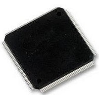
LCMXO2280C-5TN144C LATTICE SEMICONDUCTOR, LCMXO2280C-5TN144C Datasheet - Page 166

LCMXO2280C-5TN144C
Manufacturer Part Number
LCMXO2280C-5TN144C
Description
MACHXO PLD FLASH, SCRAM 1.8V, SMD
Manufacturer
LATTICE SEMICONDUCTOR
Series
MachXOr
Datasheet
1.LCMXO1200C-5TN144C.pdf
(244 pages)
Specifications of LCMXO2280C-5TN144C
Cpld Type
FLASH
No. Of Macrocells
1140
No. Of I/o's
113
Propagation Delay
3.6ns
Global Clock Setup Time
1.1ns
Frequency
600MHz
Supply Voltage Range
1.71V To 3.465V
Operating
RoHS Compliant
Available stocks
Company
Part Number
Manufacturer
Quantity
Price
Company:
Part Number:
LCMXO2280C-5TN144C
Manufacturer:
Lattice Semiconductor Corporation
Quantity:
10 000
Part Number:
LCMXO2280C-5TN144C
Manufacturer:
LATTICE/莱迪斯
Quantity:
20 000
- Current page: 166 of 244
- Download datasheet (9Mb)
MachXO sysCLOCK PLL
Lattice Semiconductor
Design and Usage Guide
nally registered by this clock. It is recommended to assert PLL RST to re-synchronize the PLL to the reference
®
clock. The LOCK signal is available to the FPGA routing to implement generation of RST. ModelSim
simulation
models take two to four reference clock cycles from RST release to LOCK high.
PLL Attributes
The PLL utilizes several attributes that allow the configuration of the PLL through source constraints. This section
details these attributes and their usage.
FIN
The input frequency can be any value within the specified frequency range based on the divider settings.
CLKI_DIV, CLKFB_DIV, CLKOP_DIV, CLKOK_DIV
These dividers determine the output frequencies of each output clock. The user is not allowed to input an invalid
combination; determined by the input frequency, the dividers, and the PLL specifications.
FREQUENCY_PIN_CLKOP, FREQUENCY_PIN_CLKOK
These output clock frequencies determine the divider values.
FDEL
The FDEL attribute is used to pass the Delay Adjustment step associated with the Output Clock of the PLL. This
allows the user to advance or retard the Output Clock by the step value passed multiplied by 250ps (nominal). The
step ranges from -8 to +8 resulting the total delay range to +/- 2ns.
PHASEADJ
The PHASEADJ attribute is used to select Coarse Phase Shift for CLKOS output. The phase adjustment is pro-
grammable in 45° increments.
DUTY
The DUTY attribute is used to select the Duty Cycle for CLKOS output. The Duty Cycle is programmable at 1/8 of
the period increment.
FB_MODE
There are three sources of feedback signals that can drive the CLKFB Divider: Internal, CLKOP (Clock Tree) and
User Clock. CLKOP (Clock Tree) feedback is used by default. Internal feedback takes the CLKOP output at CLKOP
Divider output before the Clock Tree to minimize the feedback path delay. The User Clock feedback is driven from
the dedicated pin, clock pin or user specified internal logic.
DELAY_CNTL
This attribute is designed to select the Delay Adjustment mode. If the attribute is set to “DYNAMIC” the delay con-
trol switches between Dynamic and Static depending upon the input logic of DDAMODE pin. If the attribute is set to
“STATIC”, Dynamic Delay inputs are ignored in this mode.
CLKOK Output with Lower Frequency
The CLKOK is used when a lower frequency is desired. It is a signal available for selection as a primary clock.
MachXO PLL Primitive Definitions
A PLL primitive is used for MachXO PLL implementation. The definitions of the PLL I/O ports are shown in
Table 10-2. Figure 10-4 shows the MachXO PLL primitive library symbol. The EHXPLLC includes all features avail-
able in the PLL including Dynamic Delay Adjustment.
10-4
Related parts for LCMXO2280C-5TN144C
Image
Part Number
Description
Manufacturer
Datasheet
Request
R
Part Number:
Description:
IC, CPLD, FLASH, 2280 MACROCELL FTBGA256
Manufacturer:
LATTICE SEMICONDUCTOR
Part Number:
Description:
CPLD MachXO Family 1140 Macro Cells 1.8V/2.5V/3.3V 324-Pin FTBGA Tray
Manufacturer:
LATTICE SEMICONDUCTOR
Datasheet:

Part Number:
Description:
Microcontroller Modules & Accessories MACHXO CNRL EVB
Manufacturer:
Lattice
Datasheet:

Part Number:
Description:
IC, CPLD, FLASH, 2280 MACROCELL, TQFP144
Manufacturer:
LATTICE SEMICONDUCTOR

Part Number:
Description:
MACHXO PLD FLASH, SCRAM 1.8V, SMD
Manufacturer:
LATTICE SEMICONDUCTOR
Datasheet:
Part Number:
Description:
CPLD MachXO Family 1140 Macro Cells 1.8V/2.5V/3.3V 256-Pin FTBGA Tray
Manufacturer:
LATTICE SEMICONDUCTOR
Datasheet:
Part Number:
Description:
CPLD MachXO Family 1140 Macro Cells 1.8V/2.5V/3.3V 324-Pin FTBGA Tray
Manufacturer:
LATTICE SEMICONDUCTOR
Datasheet:
Part Number:
Description:
CPLD MachXO Family 1140 Macro Cells 1.8V/2.5V/3.3V 100-Pin TQFP Tray
Manufacturer:
LATTICE SEMICONDUCTOR
Datasheet:
Part Number:
Description:
ISPLSI2032-80LT44Lattice Semiconductor [In-System Programmable High Density PLD]
Manufacturer:
Lattice Semiconductor Corp.
Datasheet:
Part Number:
Description:
IC PROGRAMMED LATTICE GAL 16V8
Manufacturer:
Lattice Semiconductor Corp.
Datasheet:
Part Number:
Description:
357-036-542-201 CARDEDGE 36POS DL .156 BLK LOPRO
Manufacturer:
Lattice Semiconductor Corp.
Datasheet:
Part Number:
Description:
357-036-542-201 CARDEDGE 36POS DL .156 BLK LOPRO
Manufacturer:
Lattice Semiconductor Corp.
Datasheet:
Part Number:
Description:
357-036-542-201 CARDEDGE 36POS DL .156 BLK LOPRO
Manufacturer:
Lattice Semiconductor Corp.
Datasheet:
Part Number:
Description:
357-036-542-201 CARDEDGE 36POS DL .156 BLK LOPRO
Manufacturer:
Lattice Semiconductor Corp.
Datasheet:


