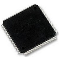
LCMXO2280C-5TN144C LATTICE SEMICONDUCTOR, LCMXO2280C-5TN144C Datasheet - Page 162

LCMXO2280C-5TN144C
Manufacturer Part Number
LCMXO2280C-5TN144C
Description
MACHXO PLD FLASH, SCRAM 1.8V, SMD
Manufacturer
LATTICE SEMICONDUCTOR
Series
MachXOr
Datasheet
1.LCMXO1200C-5TN144C.pdf
(244 pages)
Specifications of LCMXO2280C-5TN144C
Cpld Type
FLASH
No. Of Macrocells
1140
No. Of I/o's
113
Propagation Delay
3.6ns
Global Clock Setup Time
1.1ns
Frequency
600MHz
Supply Voltage Range
1.71V To 3.465V
Operating
RoHS Compliant
Available stocks
Company
Part Number
Manufacturer
Quantity
Price
Company:
Part Number:
LCMXO2280C-5TN144C
Manufacturer:
Lattice Semiconductor Corporation
Quantity:
10 000
Part Number:
LCMXO2280C-5TN144C
Manufacturer:
LATTICE/莱迪斯
Quantity:
20 000
- Current page: 162 of 244
- Download datasheet (9Mb)
Lattice Semiconductor
Appendix A. Attribute Definitions
DATA_WIDTH
Data width is associated with the RAM and FIFO elements. The DATA_WIDTH attribute defines the number of bits
in each word. It takes the values defined in the RAM size tables in each memory module.
REGMODE
REGMODE, or the Register mode attribute, is used to enable pipelining in the memory. This attribute is associated
with the RAM and FIFO elements. The REGMODE attribute takes the NOREG or OUTREG mode parameter that
disables and enables the output pipeline registers.
RESETMODE
The RESETMODE attribute allows users to select the mode of reset in the memory. This attribute is associated
with the block RAM elements. RESETMODE takes two parameters: SYNC and ASYNC. SYNC means that the
memory reset is synchronized with the clock. ASYNC means that the memory reset is asynchronous to clock.
CSDECODE
CSDECODE, or the Chip Select Decode attributes, are associated to block RAM elements. Chip Select (CS) is a
useful port when multiple cascaded EBR blocks are required by the memory. The CS signal forms the MSB for the
address when multiple EBR blocks are cascaded. CS is a 3-bit bus, so it can cascade eight memories easily.
CSDECODE takes the following parameters: “000”, “001”, “010”, “011”, “100”, “101”, “110”, and “111”. CSDECODE
values determine the decoding value of CS[2:0]. CSDECODE_W is chip select decode for write and
CSDECODE_R is chip select decode for read for Pseudo Dual Port RAM. CSDECODE_A and CSDECODE_B are
used for true dual port RAM elements and refer to the A and B ports.
WRITEMODE
The WRITEMODE attribute is associated with the block RAM elements. It takes the NORMAL, WRITETHROUGH,
and READBEFOREWRITE mode parameters.
In NORMAL mode, the output data does not change or get updated during the write operation. This mode is sup-
ported for all data widths.
In WRITETHROUGH mode, the output data is updated with the input data during the write cycle. This mode is sup-
ported for all data widths.
In READBEFOREWRITE mode, the output data port is updated with the existing data stored in the write address,
during a write cycle. This mode is supported for x9, x18 and x36 data widths.
WRITEMODE_A and WRITEMODE_B are used for dual port RAM elements and refer to the A and B ports in case
of a True Dual Port RAM.
For all modes of the True Dual Port module, simultaneous read access from one port and write access from the
other port to the same memory address is not recommended. The read data may be unknown in this situation.
Also, simultaneous write access to the same address from both ports is not recommended. When this occurs, the
data stored in the address becomes undetermined when one port tries to write a 'H' and the other tries to write a
'L'.
It is recommended that users implement control logic to identify this situation if it occurs and then either:
GSR
GSR, the Global Set/ Reset attribute, is used to enable or disable the global set/reset for the RAM element.
1. Implement status signals to flag the read data as possibly invalid, or
2. Implement control logic to prevent the simultaneous access from both ports.
9-39
Memory Usage Guide for MachXO Devices
Related parts for LCMXO2280C-5TN144C
Image
Part Number
Description
Manufacturer
Datasheet
Request
R
Part Number:
Description:
IC, CPLD, FLASH, 2280 MACROCELL FTBGA256
Manufacturer:
LATTICE SEMICONDUCTOR
Part Number:
Description:
CPLD MachXO Family 1140 Macro Cells 1.8V/2.5V/3.3V 324-Pin FTBGA Tray
Manufacturer:
LATTICE SEMICONDUCTOR
Datasheet:

Part Number:
Description:
Microcontroller Modules & Accessories MACHXO CNRL EVB
Manufacturer:
Lattice
Datasheet:

Part Number:
Description:
IC, CPLD, FLASH, 2280 MACROCELL, TQFP144
Manufacturer:
LATTICE SEMICONDUCTOR

Part Number:
Description:
MACHXO PLD FLASH, SCRAM 1.8V, SMD
Manufacturer:
LATTICE SEMICONDUCTOR
Datasheet:
Part Number:
Description:
CPLD MachXO Family 1140 Macro Cells 1.8V/2.5V/3.3V 256-Pin FTBGA Tray
Manufacturer:
LATTICE SEMICONDUCTOR
Datasheet:
Part Number:
Description:
CPLD MachXO Family 1140 Macro Cells 1.8V/2.5V/3.3V 324-Pin FTBGA Tray
Manufacturer:
LATTICE SEMICONDUCTOR
Datasheet:
Part Number:
Description:
CPLD MachXO Family 1140 Macro Cells 1.8V/2.5V/3.3V 100-Pin TQFP Tray
Manufacturer:
LATTICE SEMICONDUCTOR
Datasheet:
Part Number:
Description:
ISPLSI2032-80LT44Lattice Semiconductor [In-System Programmable High Density PLD]
Manufacturer:
Lattice Semiconductor Corp.
Datasheet:
Part Number:
Description:
IC PROGRAMMED LATTICE GAL 16V8
Manufacturer:
Lattice Semiconductor Corp.
Datasheet:
Part Number:
Description:
357-036-542-201 CARDEDGE 36POS DL .156 BLK LOPRO
Manufacturer:
Lattice Semiconductor Corp.
Datasheet:
Part Number:
Description:
357-036-542-201 CARDEDGE 36POS DL .156 BLK LOPRO
Manufacturer:
Lattice Semiconductor Corp.
Datasheet:
Part Number:
Description:
357-036-542-201 CARDEDGE 36POS DL .156 BLK LOPRO
Manufacturer:
Lattice Semiconductor Corp.
Datasheet:
Part Number:
Description:
357-036-542-201 CARDEDGE 36POS DL .156 BLK LOPRO
Manufacturer:
Lattice Semiconductor Corp.
Datasheet:


