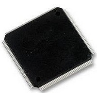
LCMXO2280C-5TN144C LATTICE SEMICONDUCTOR, LCMXO2280C-5TN144C Datasheet - Page 113

LCMXO2280C-5TN144C
Manufacturer Part Number
LCMXO2280C-5TN144C
Description
MACHXO PLD FLASH, SCRAM 1.8V, SMD
Manufacturer
LATTICE SEMICONDUCTOR
Series
MachXOr
Datasheet
1.LCMXO1200C-5TN144C.pdf
(244 pages)
Specifications of LCMXO2280C-5TN144C
Cpld Type
FLASH
No. Of Macrocells
1140
No. Of I/o's
113
Propagation Delay
3.6ns
Global Clock Setup Time
1.1ns
Frequency
600MHz
Supply Voltage Range
1.71V To 3.465V
Operating
RoHS Compliant
Available stocks
Company
Part Number
Manufacturer
Quantity
Price
Company:
Part Number:
LCMXO2280C-5TN144C
Manufacturer:
Lattice Semiconductor Corporation
Quantity:
10 000
Part Number:
LCMXO2280C-5TN144C
Manufacturer:
LATTICE/莱迪斯
Quantity:
20 000
- Current page: 113 of 244
- Download datasheet (9Mb)
Lattice Semiconductor
SLEWRATE
The SLEWRATE attribute is available for all LVTTL and LVCMOS output drivers. Each I/O pin has an individual
slew rate control. This allows designers to specify the slew rate control on pin-by-pin basis.
Values: FAST, SLOW
Default: FAST
LOC
This attribute can be used to make pin assignments to the I/O ports in the design. This attributes is only used when
the pin assignments are made in HDL source. Users can also assign pins directly using the Preference Editor GUI
in ispLEVER or the Spreadsheet View in Diamond. The appendices of this document explain this in greater detail.
Design Considerations and Usage
This section discusses some rules and considerations for designing with the MachXO sysIO buffer.
Banking Rules
• If the V
• If V
• PCI I/O standards with PCI clamps are only available on the top bank (Banks 0 and 1) on the MachXO1200 and
• PCI I/O standards with PCI clamps are not available on the MachXO640 and MachXO256 devices.
• Only 50% of the I/Os on the left and right banks of the MachXO1200 and MachXO2280 devices support a True
• All banks support emulated differential outputs using an external resistor pack and complementary LVCMOS
Zero Hold Time
The user can achieve a zero hold time for his or her inputs by specifying a zero hold time preference in the soft-
ware. The software will add additional delays to the input path in order to achieve this zero hold time.
Fast Output Path
The MachXO devices have a dedicated fast output I/O connection from the adjacent PFUs to the I/O buffers within
the PIO. This connection provides faster output delays for faster clock-to-output propagation delays and pin-to-pin
propagation delays. The software will automatically use this fast output path to achieve faster t
ments. You can fulfill the t
software.
Dedicated Pins
Global Set Rest (GSR)
The GSR in the MachXO devices is an asynchronous Global Set Reset. This signal is can be programmed to come
from either the PFU logic or from the dedicated GSR input pad. When the software does not see any logic associ-
ated with the GSR, then it will automatically use the dedicated GSR input path. This provides faster timing. When
the reset used is a logic reset, the polarity is programmable. When the dedicated GSR input from the GSR pad is
used, the polarity has to be active low.
V
thus minimizing leakage.
MachXO2280 devices.
LVDS driver. True LVDS receivers are available on all banks for the MachXO1200 and MachXO2280 devices.
driver.
CCAUX
CCIO
CCIO
, thus minimizing leakage.
for any bank is set to 1.2V, it is recommended that it be connected to the same power supply as V
for any bank is set to 3.3V, it is recommended that it be connected to the same power supply as
CO
and t
PD
requirement by assigning these preferences in the Preference Editor in the
8-10
MachXO sysIO Usage Guide
CO
and t
PD
require-
CC
,
Related parts for LCMXO2280C-5TN144C
Image
Part Number
Description
Manufacturer
Datasheet
Request
R
Part Number:
Description:
IC, CPLD, FLASH, 2280 MACROCELL FTBGA256
Manufacturer:
LATTICE SEMICONDUCTOR
Part Number:
Description:
CPLD MachXO Family 1140 Macro Cells 1.8V/2.5V/3.3V 324-Pin FTBGA Tray
Manufacturer:
LATTICE SEMICONDUCTOR
Datasheet:

Part Number:
Description:
Microcontroller Modules & Accessories MACHXO CNRL EVB
Manufacturer:
Lattice
Datasheet:

Part Number:
Description:
IC, CPLD, FLASH, 2280 MACROCELL, TQFP144
Manufacturer:
LATTICE SEMICONDUCTOR

Part Number:
Description:
MACHXO PLD FLASH, SCRAM 1.8V, SMD
Manufacturer:
LATTICE SEMICONDUCTOR
Datasheet:
Part Number:
Description:
CPLD MachXO Family 1140 Macro Cells 1.8V/2.5V/3.3V 256-Pin FTBGA Tray
Manufacturer:
LATTICE SEMICONDUCTOR
Datasheet:
Part Number:
Description:
CPLD MachXO Family 1140 Macro Cells 1.8V/2.5V/3.3V 324-Pin FTBGA Tray
Manufacturer:
LATTICE SEMICONDUCTOR
Datasheet:
Part Number:
Description:
CPLD MachXO Family 1140 Macro Cells 1.8V/2.5V/3.3V 100-Pin TQFP Tray
Manufacturer:
LATTICE SEMICONDUCTOR
Datasheet:
Part Number:
Description:
ISPLSI2032-80LT44Lattice Semiconductor [In-System Programmable High Density PLD]
Manufacturer:
Lattice Semiconductor Corp.
Datasheet:
Part Number:
Description:
IC PROGRAMMED LATTICE GAL 16V8
Manufacturer:
Lattice Semiconductor Corp.
Datasheet:
Part Number:
Description:
357-036-542-201 CARDEDGE 36POS DL .156 BLK LOPRO
Manufacturer:
Lattice Semiconductor Corp.
Datasheet:
Part Number:
Description:
357-036-542-201 CARDEDGE 36POS DL .156 BLK LOPRO
Manufacturer:
Lattice Semiconductor Corp.
Datasheet:
Part Number:
Description:
357-036-542-201 CARDEDGE 36POS DL .156 BLK LOPRO
Manufacturer:
Lattice Semiconductor Corp.
Datasheet:
Part Number:
Description:
357-036-542-201 CARDEDGE 36POS DL .156 BLK LOPRO
Manufacturer:
Lattice Semiconductor Corp.
Datasheet:


