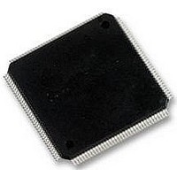
LCMXO2280C-5TN144C LATTICE SEMICONDUCTOR, LCMXO2280C-5TN144C Datasheet - Page 165

LCMXO2280C-5TN144C
Manufacturer Part Number
LCMXO2280C-5TN144C
Description
MACHXO PLD FLASH, SCRAM 1.8V, SMD
Manufacturer
LATTICE SEMICONDUCTOR
Series
MachXOr
Datasheet
1.LCMXO1200C-5TN144C.pdf
(244 pages)
Specifications of LCMXO2280C-5TN144C
Cpld Type
FLASH
No. Of Macrocells
1140
No. Of I/o's
113
Propagation Delay
3.6ns
Global Clock Setup Time
1.1ns
Frequency
600MHz
Supply Voltage Range
1.71V To 3.465V
Operating
RoHS Compliant
Available stocks
Company
Part Number
Manufacturer
Quantity
Price
Company:
Part Number:
LCMXO2280C-5TN144C
Manufacturer:
Lattice Semiconductor Corporation
Quantity:
10 000
Part Number:
LCMXO2280C-5TN144C
Manufacturer:
LATTICE/莱迪斯
Quantity:
20 000
- Current page: 165 of 244
- Download datasheet (9Mb)
Lattice Semiconductor
CLKOK Divider
The CLKOK divider feeds the global clock net. It divides the CLKOP signal of the PLL by the value of the divider. It
can be set to values of 2, 4, 6,....126,128.
PLL Inputs and Outputs
CLKI Input
The CLKI signal is the reference clock for the PLL. It must conform to the specifications in the
Sheet
routing.
RST Input
The PLL reset occurs under two conditions. At power-up an internal power-up reset signal from the configuration
block resets the PLL. The user controlled PLL reset signal RST is provided as part of the PLL module that can be
driven by an internally generated reset function or a pin. This RST signal resets all internal PLL counters. When
RST goes inactive, the PLL will start the lock-in process, and will take the t
Note: The use of RST is mandatory. RST must be asserted to start the PLL locking process or to re-start
the locking process after losing lock.
Figure 10-3 shows the timing diagram of the RST input.
Figure 10-3. RST Input Timing Diagram
CLKFB Input
The feedback signal to the PLL, which is fed through the feedback divider, can be derived from the Primary Clock
net (CLKOP), a dedicated dual-purpose pin, directly from the CLKOP divider (CLKINTFB) or from general routing.
External feedback allows the designer to compensate for board-level clock alignment.
CLKOP Output
The sysCLOCK PLL main clock output, CLKOP, is a signal available for selection as a primary clock.
CLKOS Output with Phase and Duty Cycle Select
The sysCLOCK PLL auxiliary clock output, CLKOS, is a signal available for selection as a primary clock. The
CLKOS is used when phase shift and/or duty cycle adjustment is desired. The programmable phase shift allows for
different phase in increments of 45° to 315°. The duty select feature provides duty select in 1/8th of the clock
period.
CLKOK Output with Lower Frequency
The CLKOK is used when a lower frequency is desired. It is a signal available for selection as a primary clock.
Dynamic Delay Control I/O Ports
Refer to Table 10-4 for detailed information.
LOCK Output
The LOCK output provides information about the status of the PLL. After the device is powered up and the input
clock is valid, the PLL will achieve lock within the specified lock time. Once lock is achieved, the PLL lock signal will
be asserted. If, during operation, the input clock or feedback signals to the PLL become invalid, the PLL will lose
lock. However, when the input clock completely stops, the LOCK output will remain in its last state, since it is inter-
in order for the PLL to operate correctly. The CLKI can be derived from a dedicated dual-purpose pin or from
PLL_RST
PLL_RST
LOCK
LOCK
t
RST
10-3
t
LOCK
LOCK
time to complete the PLL lock.
Design and Usage Guide
MachXO sysCLOCK PLL
MachXO Family Data
Related parts for LCMXO2280C-5TN144C
Image
Part Number
Description
Manufacturer
Datasheet
Request
R
Part Number:
Description:
IC, CPLD, FLASH, 2280 MACROCELL FTBGA256
Manufacturer:
LATTICE SEMICONDUCTOR
Part Number:
Description:
CPLD MachXO Family 1140 Macro Cells 1.8V/2.5V/3.3V 324-Pin FTBGA Tray
Manufacturer:
LATTICE SEMICONDUCTOR
Datasheet:

Part Number:
Description:
Microcontroller Modules & Accessories MACHXO CNRL EVB
Manufacturer:
Lattice
Datasheet:

Part Number:
Description:
IC, CPLD, FLASH, 2280 MACROCELL, TQFP144
Manufacturer:
LATTICE SEMICONDUCTOR

Part Number:
Description:
MACHXO PLD FLASH, SCRAM 1.8V, SMD
Manufacturer:
LATTICE SEMICONDUCTOR
Datasheet:
Part Number:
Description:
CPLD MachXO Family 1140 Macro Cells 1.8V/2.5V/3.3V 256-Pin FTBGA Tray
Manufacturer:
LATTICE SEMICONDUCTOR
Datasheet:
Part Number:
Description:
CPLD MachXO Family 1140 Macro Cells 1.8V/2.5V/3.3V 324-Pin FTBGA Tray
Manufacturer:
LATTICE SEMICONDUCTOR
Datasheet:
Part Number:
Description:
CPLD MachXO Family 1140 Macro Cells 1.8V/2.5V/3.3V 100-Pin TQFP Tray
Manufacturer:
LATTICE SEMICONDUCTOR
Datasheet:
Part Number:
Description:
ISPLSI2032-80LT44Lattice Semiconductor [In-System Programmable High Density PLD]
Manufacturer:
Lattice Semiconductor Corp.
Datasheet:
Part Number:
Description:
IC PROGRAMMED LATTICE GAL 16V8
Manufacturer:
Lattice Semiconductor Corp.
Datasheet:
Part Number:
Description:
357-036-542-201 CARDEDGE 36POS DL .156 BLK LOPRO
Manufacturer:
Lattice Semiconductor Corp.
Datasheet:
Part Number:
Description:
357-036-542-201 CARDEDGE 36POS DL .156 BLK LOPRO
Manufacturer:
Lattice Semiconductor Corp.
Datasheet:
Part Number:
Description:
357-036-542-201 CARDEDGE 36POS DL .156 BLK LOPRO
Manufacturer:
Lattice Semiconductor Corp.
Datasheet:
Part Number:
Description:
357-036-542-201 CARDEDGE 36POS DL .156 BLK LOPRO
Manufacturer:
Lattice Semiconductor Corp.
Datasheet:


