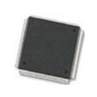
MC68376BAMFT20 Freescale Semiconductor, MC68376BAMFT20 Datasheet - Page 105

MC68376BAMFT20
Manufacturer Part Number
MC68376BAMFT20
Description
Manufacturer
Freescale Semiconductor
Datasheet
1.MC68376BAMFT20.pdf
(434 pages)
Specifications of MC68376BAMFT20
Cpu Family
68K/M683xx
Device Core
ColdFire
Device Core Size
32b
Frequency (max)
20MHz
Interface Type
QSPI/SCI
Program Memory Type
ROM
Program Memory Size
8KB
Total Internal Ram Size
7.5KB
# I/os (max)
18
Number Of Timers - General Purpose
2
Operating Supply Voltage (typ)
5V
Operating Supply Voltage (max)
5.25V
Operating Supply Voltage (min)
4.75V
On-chip Adc
16-chx10-bit
Instruction Set Architecture
RISC
Operating Temp Range
-40C to 125C
Operating Temperature Classification
Automotive
Mounting
Surface Mount
Pin Count
160
Package Type
PQFP
Lead Free Status / Rohs Status
Not Compliant
Available stocks
Company
Part Number
Manufacturer
Quantity
Price
Company:
Part Number:
MC68376BAMFT20
Manufacturer:
FREESCAL
Quantity:
245
- Current page: 105 of 434
- Download datasheet (7Mb)
5.6.2 Regular Bus Cycles
MC68336/376
USER’S MANUAL
Bus cycles terminated by DSACK assertion normally require a minimum of three CLK-
OUT cycles. To support systems that use CLKOUT to generate DSACK and other in-
puts, asynchronous input setup time and asynchronous input hold times are specified.
When these specifications are met, the MCU is guaranteed to recognize the appropri-
ate signal on a specific edge of the CLKOUT signal.
For a read cycle, when assertion of DSACK is recognized on a particular falling edge
of the clock, valid data is latched into the MCU on the next falling clock edge, provided
that the data meets the data setup time. In this case, the parameter for asynchronous
operation can be ignored.
When a system asserts DSACK for the required window around the falling edge of S2
and obeys the bus protocol by maintaining DSACK and BERR or HALT until and
throughout the clock edge that negates AS (with the appropriate asynchronous input
hold time), no wait states are inserted. The bus cycle runs at the maximum speed of
three clocks per cycle.
To ensure proper operation in a system synchronized to CLKOUT, when either BERR
or BERR and HALT is asserted after DSACK, BERR (or BERR and HALT) assertion
must satisfy the appropriate data-in setup and hold times before the falling edge of the
clock cycle after DSACK is recognized.
The following paragraphs contain a discussion of cycles that use external bus control
logic. Refer to 5.6.3 Fast Termination Cycles for information about fast termination
cycles.
To initiate a transfer, the MCU asserts an address and the SIZ[1:0] signals. The SIZ
signals and ADDR0 are externally decoded to select the active portion of the data bus.
Refer to 5.5.2 Dynamic Bus Sizing. When AS, DS, and R/W are valid, a peripheral
device either places data on the bus (read cycle) or latches data from the bus (write
cycle), then asserts a DSACK[1:0] combination that indicates port size.
The DSACK[1:0] signals can be asserted before the data from a peripheral device is
valid on a read cycle. To ensure valid data is latched into the MCU, a maximum period
between DSACK assertion and DS assertion is specified.
There is no specified maximum for the period between the assertion of AS and
DSACK. Although the MCU can transfer data in a minimum of three clock cycles when
the cycle is terminated with DSACK, the MCU inserts wait cycles in clock period incre-
ments until either DSACK signal goes low.
SYSTEM INTEGRATION MODULE
MOTOROLA
5-27
Related parts for MC68376BAMFT20
Image
Part Number
Description
Manufacturer
Datasheet
Request
R
Part Number:
Description:
Manufacturer:
Freescale Semiconductor, Inc
Datasheet:
Part Number:
Description:
Manufacturer:
Freescale Semiconductor, Inc
Datasheet:
Part Number:
Description:
Manufacturer:
Freescale Semiconductor, Inc
Datasheet:
Part Number:
Description:
Manufacturer:
Freescale Semiconductor, Inc
Datasheet:
Part Number:
Description:
Manufacturer:
Freescale Semiconductor, Inc
Datasheet:
Part Number:
Description:
Manufacturer:
Freescale Semiconductor, Inc
Datasheet:
Part Number:
Description:
Manufacturer:
Freescale Semiconductor, Inc
Datasheet:
Part Number:
Description:
Manufacturer:
Freescale Semiconductor, Inc
Datasheet:
Part Number:
Description:
Manufacturer:
Freescale Semiconductor, Inc
Datasheet:
Part Number:
Description:
Manufacturer:
Freescale Semiconductor, Inc
Datasheet:
Part Number:
Description:
Manufacturer:
Freescale Semiconductor, Inc
Datasheet:
Part Number:
Description:
Manufacturer:
Freescale Semiconductor, Inc
Datasheet:
Part Number:
Description:
Manufacturer:
Freescale Semiconductor, Inc
Datasheet:
Part Number:
Description:
Manufacturer:
Freescale Semiconductor, Inc
Datasheet:
Part Number:
Description:
Manufacturer:
Freescale Semiconductor, Inc
Datasheet:


