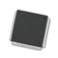
MC68376BAMFT20 Freescale Semiconductor, MC68376BAMFT20 Datasheet - Page 285

MC68376BAMFT20
Manufacturer Part Number
MC68376BAMFT20
Description
Manufacturer
Freescale Semiconductor
Datasheet
1.MC68376BAMFT20.pdf
(434 pages)
Specifications of MC68376BAMFT20
Cpu Family
68K/M683xx
Device Core
ColdFire
Device Core Size
32b
Frequency (max)
20MHz
Interface Type
QSPI/SCI
Program Memory Type
ROM
Program Memory Size
8KB
Total Internal Ram Size
7.5KB
# I/os (max)
18
Number Of Timers - General Purpose
2
Operating Supply Voltage (typ)
5V
Operating Supply Voltage (max)
5.25V
Operating Supply Voltage (min)
4.75V
On-chip Adc
16-chx10-bit
Instruction Set Architecture
RISC
Operating Temp Range
-40C to 125C
Operating Temperature Classification
Automotive
Mounting
Surface Mount
Pin Count
160
Package Type
PQFP
Lead Free Status / Rohs Status
Not Compliant
Available stocks
Company
Part Number
Manufacturer
Quantity
Price
Company:
Part Number:
MC68376BAMFT20
Manufacturer:
FREESCAL
Quantity:
245
- Current page: 285 of 434
- Download datasheet (7Mb)
MC68336/376
USER’S MANUAL
Num
NOTES:
10. If the asynchronous setup time (specification 47A) requirements are satisfied, the DSACK[1:0] low to data setup
11. To ensure coherency during every operand transfer, BG will not be asserted in response to BR until after all
12. In the absence of DSACK[1:0], BERR is an asynchronous input using the asynchronous setup time (specification
13. After external RESET negation is detected, a short transition period (approximately 2 t
14. External assertion of the RESET input can overlap internally-generated resets. To insure that an external
15. External logic must pull RESET high during this period in order for normal MCU operation to begin.
76
77
78
1. All AC timing is shown with respect to 20% V
2. The base configuration of the MC68336/376 requires a 20.97 MHz crystal reference.
3. When an external clock is used, minimum high and low times are based on a 50% duty cycle. The minimum
4. Parameters for an external clock signal applied while the internal PLL is disabled (MODCLK pin held low during
5. Address access time = (2.5 + WS) t
6. Specification 9A is the worst-case skew between AS and DS or CS. The amount of skew depends on the relative
7. If multiple chip selects are used, CS width negated (specification 15) applies to the time from the negation of a
8. Hold times are specified with respect to DS or CS on asynchronous reads and with respect to CLKOUT on fast
9. Maximum value is equal to (t
time (specification 31) and DSACK[1:0] low to BERR low setup time (specification 48) can be ignored. The data
must only satisfy the data-in to clock low setup time (specification 27) for the following clock cycle. BERR must
satisfy only the late BERR low to clock low setup time (specification 27A) for the following clock cycle.
cycles of the current operand transfer are complete and RMC is negated.
47A).
drives RESET low for 512 t
reset is recognized in all cases, RESET must be asserted for at least 590 CLKOUT cycles.
allowable t
external clock input duty cycle and minimum t
reset). Does not pertain to an external VCO reference applied while the PLL is enabled (MODCLK pin held high
during reset). When the PLL is enabled, the clock synthesizer detects successive transitions of the reference
signal. If transitions occur within the correct clock period, rise/fall times and duty cycle are not critical.
Chip select access time = (2 + WS) t
Where: WS = number of wait states. When fast termination is used (2 clock bus) WS = –1.
loading of these signals. When loads are kept within specified limits, skew will not cause AS and DS to fall outside
the limits shown in specification 9.
heavily loaded chip select to the assertion of a lightly loaded chip select. The CS width negated specification
between multiple chip selects does not apply to chip selects being used for synchronous ECLK cycles.
cycle reads. The user is free to use either hold time.
Mode Select Hold Time
RESET Assertion Time
RESET Rise Time
Xcyc
period is reduced when the duty cycle of the external clock signal varies. The relationship between
Minimum t
(V
DD
14
and V
,
15
Xcyc
13
cyc
Table A-6 AC Timing (Continued)
cyc
.
DDSYN
period = minimum t
ELECTRICAL CHARACTERISTICS
/ 2) + 25 ns.
Characteristic
cyc
cyc
= 5.0 Vdc 5%, V
– t
– t
CHAV
LSA
DD
Xcyc
– t
– t
and 70% V
DICL
XCHL
DICL
is expressed:
/ (50% –external clock input duty cycle tolerance).
SS
DD
= 0 Vdc, T
levels unless otherwise noted.
A
= T
L
to T
Symbol
t
t
t
RSTA
RSTR
MSH
H
)
cyc
1
) elapses, then the SIM
Min
—
0
4
MOTOROLA
Max
10
—
—
Unit
t
t
ns
cyc
cyc
A-9
Related parts for MC68376BAMFT20
Image
Part Number
Description
Manufacturer
Datasheet
Request
R
Part Number:
Description:
Manufacturer:
Freescale Semiconductor, Inc
Datasheet:
Part Number:
Description:
Manufacturer:
Freescale Semiconductor, Inc
Datasheet:
Part Number:
Description:
Manufacturer:
Freescale Semiconductor, Inc
Datasheet:
Part Number:
Description:
Manufacturer:
Freescale Semiconductor, Inc
Datasheet:
Part Number:
Description:
Manufacturer:
Freescale Semiconductor, Inc
Datasheet:
Part Number:
Description:
Manufacturer:
Freescale Semiconductor, Inc
Datasheet:
Part Number:
Description:
Manufacturer:
Freescale Semiconductor, Inc
Datasheet:
Part Number:
Description:
Manufacturer:
Freescale Semiconductor, Inc
Datasheet:
Part Number:
Description:
Manufacturer:
Freescale Semiconductor, Inc
Datasheet:
Part Number:
Description:
Manufacturer:
Freescale Semiconductor, Inc
Datasheet:
Part Number:
Description:
Manufacturer:
Freescale Semiconductor, Inc
Datasheet:
Part Number:
Description:
Manufacturer:
Freescale Semiconductor, Inc
Datasheet:
Part Number:
Description:
Manufacturer:
Freescale Semiconductor, Inc
Datasheet:
Part Number:
Description:
Manufacturer:
Freescale Semiconductor, Inc
Datasheet:
Part Number:
Description:
Manufacturer:
Freescale Semiconductor, Inc
Datasheet:


