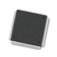
MC68376BAMFT20 Freescale Semiconductor, MC68376BAMFT20 Datasheet - Page 108

MC68376BAMFT20
Manufacturer Part Number
MC68376BAMFT20
Description
Manufacturer
Freescale Semiconductor
Datasheet
1.MC68376BAMFT20.pdf
(434 pages)
Specifications of MC68376BAMFT20
Cpu Family
68K/M683xx
Device Core
ColdFire
Device Core Size
32b
Frequency (max)
20MHz
Interface Type
QSPI/SCI
Program Memory Type
ROM
Program Memory Size
8KB
Total Internal Ram Size
7.5KB
# I/os (max)
18
Number Of Timers - General Purpose
2
Operating Supply Voltage (typ)
5V
Operating Supply Voltage (max)
5.25V
Operating Supply Voltage (min)
4.75V
On-chip Adc
16-chx10-bit
Instruction Set Architecture
RISC
Operating Temp Range
-40C to 125C
Operating Temperature Classification
Automotive
Mounting
Surface Mount
Pin Count
160
Package Type
PQFP
Lead Free Status / Rohs Status
Not Compliant
Available stocks
Company
Part Number
Manufacturer
Quantity
Price
Company:
Part Number:
MC68376BAMFT20
Manufacturer:
FREESCAL
Quantity:
245
- Current page: 108 of 434
- Download datasheet (7Mb)
5.6.3 Fast Termination Cycles
5.6.4 CPU Space Cycles
5-30
MOTOROLA
When an external device has a fast access time, the chip-select circuit fast termination
option can provide a two-cycle external bus transfer. Because the chip-select circuits
are driven from the system clock, the bus cycle termination is inherently synchronized
with the system clock.
If multiple chip-selects are to be used to provide control signals to a single device and
match conditions occur simultaneously, all MODE, STRB, and associated DSACK
fields must be programmed to the same value. This prevents a conflict on the internal
bus when the wait states are loaded into the DSACK counter shared by all chip-
selects.
Fast termination cycles use internal handshaking signals generated by the chip-select
logic. To initiate a transfer, the MCU asserts an address and the SIZ[1:0] signals.
When AS, DS, and R/W are valid, a peripheral device either places data on the bus
(read cycle) or latches data from the bus (write cycle). At the appropriate time, chip-
select logic asserts data and size acknowledge signals.
The DSACK option fields in the chip-select option registers determine whether inter-
nally generated DSACK or externally generated DSACK is used. The external DSACK
lines are always active, regardless of the setting of the DSACK field in the chip-select
option registers. Thus, an external DSACK can always terminate a bus cycle. Holding
a DSACK line low will cause all external bus cycles to be three-cycle (zero wait states)
accesses unless the chip-select option register specifies fast accesses.
For fast termination cycles, the fast termination encoding (%1110) must be used. Re-
fer to 5.9.1 Chip-Select Registers for information about fast termination setup.
To use fast termination, an external device must be fast enough to have data ready
within the specified setup time (for example, by the falling edge of S4). Refer to Table
A-6 and Figures A-6 and A-7 for information about fast termination timing.
When fast termination is in use, DS is asserted during read cycles but not during write
cycles. The STRB field in the chip-select option register used must be programmed
with the address strobe encoding to assert the chip-select signal for a fast termination
write.
Function code signals FC[2:0] designate which of eight external address spaces is ac-
cessed during a bus cycle. Address space 7 is designated CPU space. CPU space is
used for control information not normally associated with read or write bus cycles.
Function codes are valid only while AS is asserted. Refer to 5.5.1.7 Function Codes
for more information on codes and encoding.
During a CPU space access, ADDR[19:16] are encoded to reflect the type of access
being made. Figure 5-12 shows the three encodings used by 68300 family microcon-
trollers. These encodings represent breakpoint acknowledge (Type $0) cycles, low
power stop broadcast (Type $3) cycles, and interrupt acknowledge (Type $F) cycles.
Refer to 5.8 Interrupts for information about interrupt acknowledge bus cycles.
SYSTEM INTEGRATION MODULE
USER’S MANUAL
MC68336/376
Related parts for MC68376BAMFT20
Image
Part Number
Description
Manufacturer
Datasheet
Request
R
Part Number:
Description:
Manufacturer:
Freescale Semiconductor, Inc
Datasheet:
Part Number:
Description:
Manufacturer:
Freescale Semiconductor, Inc
Datasheet:
Part Number:
Description:
Manufacturer:
Freescale Semiconductor, Inc
Datasheet:
Part Number:
Description:
Manufacturer:
Freescale Semiconductor, Inc
Datasheet:
Part Number:
Description:
Manufacturer:
Freescale Semiconductor, Inc
Datasheet:
Part Number:
Description:
Manufacturer:
Freescale Semiconductor, Inc
Datasheet:
Part Number:
Description:
Manufacturer:
Freescale Semiconductor, Inc
Datasheet:
Part Number:
Description:
Manufacturer:
Freescale Semiconductor, Inc
Datasheet:
Part Number:
Description:
Manufacturer:
Freescale Semiconductor, Inc
Datasheet:
Part Number:
Description:
Manufacturer:
Freescale Semiconductor, Inc
Datasheet:
Part Number:
Description:
Manufacturer:
Freescale Semiconductor, Inc
Datasheet:
Part Number:
Description:
Manufacturer:
Freescale Semiconductor, Inc
Datasheet:
Part Number:
Description:
Manufacturer:
Freescale Semiconductor, Inc
Datasheet:
Part Number:
Description:
Manufacturer:
Freescale Semiconductor, Inc
Datasheet:
Part Number:
Description:
Manufacturer:
Freescale Semiconductor, Inc
Datasheet:


