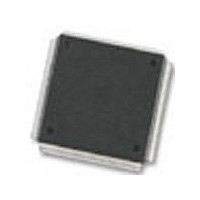
MC68376BAMFT20 Freescale Semiconductor, MC68376BAMFT20 Datasheet - Page 236

MC68376BAMFT20
Manufacturer Part Number
MC68376BAMFT20
Description
Manufacturer
Freescale Semiconductor
Datasheet
1.MC68376BAMFT20.pdf
(434 pages)
Specifications of MC68376BAMFT20
Cpu Family
68K/M683xx
Device Core
ColdFire
Device Core Size
32b
Frequency (max)
20MHz
Interface Type
QSPI/SCI
Program Memory Type
ROM
Program Memory Size
8KB
Total Internal Ram Size
7.5KB
# I/os (max)
18
Number Of Timers - General Purpose
2
Operating Supply Voltage (typ)
5V
Operating Supply Voltage (max)
5.25V
Operating Supply Voltage (min)
4.75V
On-chip Adc
16-chx10-bit
Instruction Set Architecture
RISC
Operating Temp Range
-40C to 125C
Operating Temperature Classification
Automotive
Mounting
Surface Mount
Pin Count
160
Package Type
PQFP
Lead Free Status / Rohs Status
Not Compliant
Available stocks
Company
Part Number
Manufacturer
Quantity
Price
Company:
Part Number:
MC68376BAMFT20
Manufacturer:
FREESCAL
Quantity:
245
- Current page: 236 of 434
- Download datasheet (7Mb)
11.2 TPU Components
11.2.1 Time Bases
11.2.2 Timer Channels
11-2
MOTOROLA
The G mask set (or motion control mask set) includes the following functions:
The TPU consists of two 16-bit time bases, sixteen independent timer channels, a task
scheduler, a microengine, and a host interface. In addition, a dual-ported parameter
RAM is used to pass parameters between the module and the CPU32.
Two 16-bit counters provide reference time bases for all output compare and input
capture events. Prescalers for both time bases are controlled by the CPU32 via bit
fields in the TPU module configuration register (TPUMCR). Timer count registers
TCR1 and TCR2 provide access to the current counter values. TCR1 and TCR2 can
be read by TPU microcode, but are not directly available to the CPU32. The TCR1
clock is derived from the system clock. The TCR2 clock can be derived from the sys-
tem clock or from an external clock input via the T2CLK pin.
The TPU has 16 independent channels, each connected to an MCU pin. The channels
have identical hardware. Each channel consists of an event register and pin control
logic. The event register contains a 16-bit capture register, a 16-bit compare/match
register, and a 16-bit greater-than-or-equal-to comparator. The direction of each pin,
either output or input, is determined by the TPU microengine. Each channel can either
use the same time base for match and capture, or can use one time base for match
and the other for capture.
• Synchronized pulse width modulation
• Period measurement with additional transition detect
• Period measurement with missing transition detect
• Position-synchronized pulse generator
• Stepper motor
• Period/pulse width accumulator
• Quadrature decode
• Table stepper motor
• New input capture/transition counter
• Queued output match
• Programmable time accumulator
• Multichannel pulse width modulation
• Fast quadrature decode
• Universal asynchronous receiver/transmitter
• Brushless motor communication
• Frequency measurement
• Hall effect decode
TIME PROCESSOR UNIT
USER’S MANUAL
MC68336/376
Related parts for MC68376BAMFT20
Image
Part Number
Description
Manufacturer
Datasheet
Request
R
Part Number:
Description:
Manufacturer:
Freescale Semiconductor, Inc
Datasheet:
Part Number:
Description:
Manufacturer:
Freescale Semiconductor, Inc
Datasheet:
Part Number:
Description:
Manufacturer:
Freescale Semiconductor, Inc
Datasheet:
Part Number:
Description:
Manufacturer:
Freescale Semiconductor, Inc
Datasheet:
Part Number:
Description:
Manufacturer:
Freescale Semiconductor, Inc
Datasheet:
Part Number:
Description:
Manufacturer:
Freescale Semiconductor, Inc
Datasheet:
Part Number:
Description:
Manufacturer:
Freescale Semiconductor, Inc
Datasheet:
Part Number:
Description:
Manufacturer:
Freescale Semiconductor, Inc
Datasheet:
Part Number:
Description:
Manufacturer:
Freescale Semiconductor, Inc
Datasheet:
Part Number:
Description:
Manufacturer:
Freescale Semiconductor, Inc
Datasheet:
Part Number:
Description:
Manufacturer:
Freescale Semiconductor, Inc
Datasheet:
Part Number:
Description:
Manufacturer:
Freescale Semiconductor, Inc
Datasheet:
Part Number:
Description:
Manufacturer:
Freescale Semiconductor, Inc
Datasheet:
Part Number:
Description:
Manufacturer:
Freescale Semiconductor, Inc
Datasheet:
Part Number:
Description:
Manufacturer:
Freescale Semiconductor, Inc
Datasheet:


