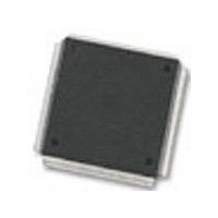
MC68376BAMFT20 Freescale Semiconductor, MC68376BAMFT20 Datasheet - Page 212

MC68376BAMFT20
Manufacturer Part Number
MC68376BAMFT20
Description
Manufacturer
Freescale Semiconductor
Datasheet
1.MC68376BAMFT20.pdf
(434 pages)
Specifications of MC68376BAMFT20
Cpu Family
68K/M683xx
Device Core
ColdFire
Device Core Size
32b
Frequency (max)
20MHz
Interface Type
QSPI/SCI
Program Memory Type
ROM
Program Memory Size
8KB
Total Internal Ram Size
7.5KB
# I/os (max)
18
Number Of Timers - General Purpose
2
Operating Supply Voltage (typ)
5V
Operating Supply Voltage (max)
5.25V
Operating Supply Voltage (min)
4.75V
On-chip Adc
16-chx10-bit
Instruction Set Architecture
RISC
Operating Temp Range
-40C to 125C
Operating Temperature Classification
Automotive
Mounting
Surface Mount
Pin Count
160
Package Type
PQFP
Lead Free Status / Rohs Status
Not Compliant
Available stocks
Company
Part Number
Manufacturer
Quantity
Price
Company:
Part Number:
MC68376BAMFT20
Manufacturer:
FREESCAL
Quantity:
245
- Current page: 212 of 434
- Download datasheet (7Mb)
8-30
MOTOROLA
To prepare the QADC for a scan sequence, the desired channel conversions are writ-
ten to the CCW table. Software establishes the criteria for initiating the queue execu-
tion by programming queue operating mode. The queue operating mode determines
what type of trigger event initiates queue execution.
A scan sequence may be initiated by the following trigger events:
Software also specifies whether the QADC is to perform a single pass through the
queue or is to scan continuously. When a single-scan mode is selected, queue execu-
tion begins when software sets the single-scan enable bit. When a continuous-scan
mode is selected, the queue remains active in the selected queue operating mode af-
ter the QADC completes each queue scan sequence.
During queue execution, the QADC reads each CCW from the active queue and exe-
cutes conversions in four stages:
During initial sample, the selected input channel is connected to the sample capacitor
at the input of the sample buffer amplifier.
During the transfer period, the sample capacitor is disconnected from the multiplexer,
and the stored voltage is buffered and transferred to the RC DAC array.
During the final sample period, the sample capacitor and amplifier are bypassed, and
the multiplexer input charges the RC DAC array directly. Each CCW specifies a final
input sample time of 2, 4, 8, or 16 QCLK cycles. When an analog-to-digital conversion
is complete, the result is written to the corresponding location in the result word table.
The QADC continues to sequentially execute each CCW in the queue until the end of
the queue is detected or a pause bit is found in a CCW.
When the pause bit is set in the current CCW, the QADC stops execution of the queue
until a new trigger event occurs. The pause status flag bit is set, which may generate
an interrupt request to notify software that the queue has reached the pause state.
When the next trigger event occurs, the paused state ends, and the QADC continues
to execute each CCW in the queue until another pause is encountered or the end of
the queue is detected.
An end-of-queue condition is indicated as follows:
• A software command
• Expiration of the periodic/interval timer
• An external trigger signal
1. Initial sample
2. Transfer
3. Final sample
4. Resolution
• The CCW channel field is programmed with 63 ($3F) to specify the end of the
• The end of queue 1 is implied by the beginning of queue 2, which is specified in
• The physical end of the queue RAM space defines the end of either queue.
the BQ2 field in QACR2.
queue.
QUEUED ANALOG-TO-DIGITAL CONVERTER MODULE
USER’S MANUAL
MC68336/376
Related parts for MC68376BAMFT20
Image
Part Number
Description
Manufacturer
Datasheet
Request
R
Part Number:
Description:
Manufacturer:
Freescale Semiconductor, Inc
Datasheet:
Part Number:
Description:
Manufacturer:
Freescale Semiconductor, Inc
Datasheet:
Part Number:
Description:
Manufacturer:
Freescale Semiconductor, Inc
Datasheet:
Part Number:
Description:
Manufacturer:
Freescale Semiconductor, Inc
Datasheet:
Part Number:
Description:
Manufacturer:
Freescale Semiconductor, Inc
Datasheet:
Part Number:
Description:
Manufacturer:
Freescale Semiconductor, Inc
Datasheet:
Part Number:
Description:
Manufacturer:
Freescale Semiconductor, Inc
Datasheet:
Part Number:
Description:
Manufacturer:
Freescale Semiconductor, Inc
Datasheet:
Part Number:
Description:
Manufacturer:
Freescale Semiconductor, Inc
Datasheet:
Part Number:
Description:
Manufacturer:
Freescale Semiconductor, Inc
Datasheet:
Part Number:
Description:
Manufacturer:
Freescale Semiconductor, Inc
Datasheet:
Part Number:
Description:
Manufacturer:
Freescale Semiconductor, Inc
Datasheet:
Part Number:
Description:
Manufacturer:
Freescale Semiconductor, Inc
Datasheet:
Part Number:
Description:
Manufacturer:
Freescale Semiconductor, Inc
Datasheet:
Part Number:
Description:
Manufacturer:
Freescale Semiconductor, Inc
Datasheet:


