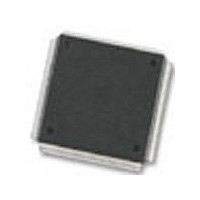
MC68376BAMFT20 Freescale Semiconductor, MC68376BAMFT20 Datasheet - Page 120

MC68376BAMFT20
Manufacturer Part Number
MC68376BAMFT20
Description
Manufacturer
Freescale Semiconductor
Datasheet
1.MC68376BAMFT20.pdf
(434 pages)
Specifications of MC68376BAMFT20
Cpu Family
68K/M683xx
Device Core
ColdFire
Device Core Size
32b
Frequency (max)
20MHz
Interface Type
QSPI/SCI
Program Memory Type
ROM
Program Memory Size
8KB
Total Internal Ram Size
7.5KB
# I/os (max)
18
Number Of Timers - General Purpose
2
Operating Supply Voltage (typ)
5V
Operating Supply Voltage (max)
5.25V
Operating Supply Voltage (min)
4.75V
On-chip Adc
16-chx10-bit
Instruction Set Architecture
RISC
Operating Temp Range
-40C to 125C
Operating Temperature Classification
Automotive
Mounting
Surface Mount
Pin Count
160
Package Type
PQFP
Lead Free Status / Rohs Status
Not Compliant
Available stocks
Company
Part Number
Manufacturer
Quantity
Price
Company:
Part Number:
MC68376BAMFT20
Manufacturer:
FREESCAL
Quantity:
245
- Current page: 120 of 434
- Download datasheet (7Mb)
5.7.3.1 Data Bus Mode Selection
5-42
MOTOROLA
All data lines have weak internal pull-up drivers. When pins are held high by the inter-
nal drivers, the MCU uses a default operating configuration. However, specific lines
can be held low externally during reset to achieve an alternate configuration.
Use an active device to hold data bus lines low. Data bus configuration logic must re-
lease the bus before the first bus cycle after reset to prevent conflict with external
memory devices. The first bus cycle occurs ten CLKOUT cycles after RESET is re-
leased. If external mode selection logic causes a conflict of this type, an isolation re-
sistor on the driven lines may be required. Figure 5-16 shows a recommended method
for conditioning the mode select signals.
The mode configuration drivers are conditioned with R/W and DS to prevent conflicts
between external devices and the MCU when reset is asserted. If external RESET is
asserted during an external write cycle, R/W conditioning (as shown in Figure 5-16)
prevents corruption of the data during the write. Similarly, DS conditions the mode con-
figuration drivers so that external reads are not corrupted when RESET is asserted
during an external read cycle.
NOTES:
1. The DATA11 bus must remain high during reset to ensure normal operation.
Mode Select Pin
MODCLK
DATA11
DATA0
DATA1
DATA2
DATA3
DATA4
DATA5
DATA6
DATA7
DATA8
DATA9
BKPT
External bus loading can overcome the weak internal pull-up drivers
on data bus lines and hold pins low during reset.
SYSTEM INTEGRATION MODULE
Table 5-15 Reset Mode Selection
Background mode disabled
AVEC, DS, AS, SIZ[1:0]
VCO = System clock
Normal operation
Default Function
CSBOOT 16-bit
(Pin Left High)
DSACK[1:0],
MODCLK
CS[10:6]
IRQ[7:1]
CS[7:6]
CS[8:6]
CS[9:6]
CS0
CS1
CS2
CS3
CS4
CS5
CS6
NOTE
1
Background mode enabled
EXTAL = System clock
Alternate Function
(Pin Pulled Low)
CSBOOT 8-bit
ADDR[20:19]
ADDR[21:19]
ADDR[22:19]
ADDR[23:19]
Reserved
ADDR19
BGACK
PORTE
PORTF
FC0
FC1
FC2
BR
BG
USER’S MANUAL
MC68336/376
Related parts for MC68376BAMFT20
Image
Part Number
Description
Manufacturer
Datasheet
Request
R
Part Number:
Description:
Manufacturer:
Freescale Semiconductor, Inc
Datasheet:
Part Number:
Description:
Manufacturer:
Freescale Semiconductor, Inc
Datasheet:
Part Number:
Description:
Manufacturer:
Freescale Semiconductor, Inc
Datasheet:
Part Number:
Description:
Manufacturer:
Freescale Semiconductor, Inc
Datasheet:
Part Number:
Description:
Manufacturer:
Freescale Semiconductor, Inc
Datasheet:
Part Number:
Description:
Manufacturer:
Freescale Semiconductor, Inc
Datasheet:
Part Number:
Description:
Manufacturer:
Freescale Semiconductor, Inc
Datasheet:
Part Number:
Description:
Manufacturer:
Freescale Semiconductor, Inc
Datasheet:
Part Number:
Description:
Manufacturer:
Freescale Semiconductor, Inc
Datasheet:
Part Number:
Description:
Manufacturer:
Freescale Semiconductor, Inc
Datasheet:
Part Number:
Description:
Manufacturer:
Freescale Semiconductor, Inc
Datasheet:
Part Number:
Description:
Manufacturer:
Freescale Semiconductor, Inc
Datasheet:
Part Number:
Description:
Manufacturer:
Freescale Semiconductor, Inc
Datasheet:
Part Number:
Description:
Manufacturer:
Freescale Semiconductor, Inc
Datasheet:
Part Number:
Description:
Manufacturer:
Freescale Semiconductor, Inc
Datasheet:


