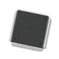
MC68376BAMFT20 Freescale Semiconductor, MC68376BAMFT20 Datasheet - Page 227

MC68376BAMFT20
Manufacturer Part Number
MC68376BAMFT20
Description
Manufacturer
Freescale Semiconductor
Datasheet
1.MC68376BAMFT20.pdf
(434 pages)
Specifications of MC68376BAMFT20
Cpu Family
68K/M683xx
Device Core
ColdFire
Device Core Size
32b
Frequency (max)
20MHz
Interface Type
QSPI/SCI
Program Memory Type
ROM
Program Memory Size
8KB
Total Internal Ram Size
7.5KB
# I/os (max)
18
Number Of Timers - General Purpose
2
Operating Supply Voltage (typ)
5V
Operating Supply Voltage (max)
5.25V
Operating Supply Voltage (min)
4.75V
On-chip Adc
16-chx10-bit
Instruction Set Architecture
RISC
Operating Temp Range
-40C to 125C
Operating Temperature Classification
Automotive
Mounting
Surface Mount
Pin Count
160
Package Type
PQFP
Lead Free Status / Rohs Status
Not Compliant
Available stocks
Company
Part Number
Manufacturer
Quantity
Price
Company:
Part Number:
MC68376BAMFT20
Manufacturer:
FREESCAL
Quantity:
245
- Current page: 227 of 434
- Download datasheet (7Mb)
MC68336/376
USER’S MANUAL
ator, though internally, channel B has two data registers (B1 and B2). DASM operating
mode determines which register is software accessible. Refer to Table 10-3.
Register contents are always transferred automatically at the correct time so that the
minimum pulse (measured or generated) is just one time base bus count. The A and
B data registers are always read/write registers, accessible via the CTM4 submodule
bus.
The CTM4 has four DASMs. Figure 10-5 shows a block diagram of the DASM.
Output Pulse Width
Modulation Mode
Output Compare
(IPWM, IPM, IC)
(OCA, OCAB)
SELECT
Input Capture
BUS
(OPWM)
Mode
MODE3 MODE2
CONTROL REGISTER BITS
16-BIT COMPARATOR A
16-BIT COMPARATOR B
16-BIT REGISTER B2
16-BIT REGISTER B1
16-BIT REGISTER A
BSL
Table 10-3 Channel B Data Register Access
REGISTER B
MODE1 MODE0
Registers A and B2 are used to hold the captured values. In these modes,
the B1 register is used as a temporary latch for channel B.
Registers A and B2 are used to define the output pulse. Register B1 is not
used in these modes.
Registers A and B1 are used as primary registers and hidden register B2 is
used as a double buffer for channel B.
Figure 10-5 DASM Block Diagram
CONFIGURABLE TIMER MODULE 4
2 TIME BASE BUSES
SUBMODULE BUS
FORCA
FLIP-FLOP
Data Register
OUTPUT
FLAG
FORCB
CONTROL REGISTER BITS
IL2
INTERRUPT
CONTROL
OUTPUT
BUFFER
DETECT
EDPOL
EDGE
WOR
IL1
IL0
IARB3
I/O PIN
IN
TBBA
TBBB
MOTOROLA
CTM DASM BLOCK
10-11
Related parts for MC68376BAMFT20
Image
Part Number
Description
Manufacturer
Datasheet
Request
R
Part Number:
Description:
Manufacturer:
Freescale Semiconductor, Inc
Datasheet:
Part Number:
Description:
Manufacturer:
Freescale Semiconductor, Inc
Datasheet:
Part Number:
Description:
Manufacturer:
Freescale Semiconductor, Inc
Datasheet:
Part Number:
Description:
Manufacturer:
Freescale Semiconductor, Inc
Datasheet:
Part Number:
Description:
Manufacturer:
Freescale Semiconductor, Inc
Datasheet:
Part Number:
Description:
Manufacturer:
Freescale Semiconductor, Inc
Datasheet:
Part Number:
Description:
Manufacturer:
Freescale Semiconductor, Inc
Datasheet:
Part Number:
Description:
Manufacturer:
Freescale Semiconductor, Inc
Datasheet:
Part Number:
Description:
Manufacturer:
Freescale Semiconductor, Inc
Datasheet:
Part Number:
Description:
Manufacturer:
Freescale Semiconductor, Inc
Datasheet:
Part Number:
Description:
Manufacturer:
Freescale Semiconductor, Inc
Datasheet:
Part Number:
Description:
Manufacturer:
Freescale Semiconductor, Inc
Datasheet:
Part Number:
Description:
Manufacturer:
Freescale Semiconductor, Inc
Datasheet:
Part Number:
Description:
Manufacturer:
Freescale Semiconductor, Inc
Datasheet:
Part Number:
Description:
Manufacturer:
Freescale Semiconductor, Inc
Datasheet:


