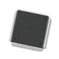
MC68376BAMFT20 Freescale Semiconductor, MC68376BAMFT20 Datasheet - Page 45

MC68376BAMFT20
Manufacturer Part Number
MC68376BAMFT20
Description
Manufacturer
Freescale Semiconductor
Datasheet
1.MC68376BAMFT20.pdf
(434 pages)
Specifications of MC68376BAMFT20
Cpu Family
68K/M683xx
Device Core
ColdFire
Device Core Size
32b
Frequency (max)
20MHz
Interface Type
QSPI/SCI
Program Memory Type
ROM
Program Memory Size
8KB
Total Internal Ram Size
7.5KB
# I/os (max)
18
Number Of Timers - General Purpose
2
Operating Supply Voltage (typ)
5V
Operating Supply Voltage (max)
5.25V
Operating Supply Voltage (min)
4.75V
On-chip Adc
16-chx10-bit
Instruction Set Architecture
RISC
Operating Temp Range
-40C to 125C
Operating Temperature Classification
Automotive
Mounting
Surface Mount
Pin Count
160
Package Type
PQFP
Lead Free Status / Rohs Status
Not Compliant
Available stocks
Company
Part Number
Manufacturer
Quantity
Price
Company:
Part Number:
MC68376BAMFT20
Manufacturer:
FREESCAL
Quantity:
245
- Current page: 45 of 434
- Download datasheet (7Mb)
MC68336/376
USER’S MANUAL
DSI, DSO, DSCLK
AN[59:48]/[3:0]
CTD[10:9]/[4:3]
EXTAL, XTAL
AN[w, x, y, z]
DSACK[1:0]
ADDR[23:0]
DATA[15:0]
CPWM[8:5]
ETRIG[2:1]
Mnemonic
CSBOOT
MODCLK
CLKOUT
CANRX0
PCS[3:0]
CANTX0
CS[10:0]
FREEZE
IRQ[7:1]
IFETCH
BGACK
CTM2C
MA[2:0]
PC[6:0]
FC[2:0]
PE[7:0]
PF[7:0]
AVEC
BERR
BKPT
ECLK
HALT
IPIPE
MISO
MOSI
BG
BR
DS
AS
Developmental Serial In,
Bus Grant Acknowledge
Peripheral Chip-Selects
TouCAN Transmit Data
QADC External Trigger
TouCAN Receive Data
CTM4 Modulus Clock
CTM4 Double Action
Master In, Slave Out
Master Out, Slave In
QADC Analog Input
QADC Analog Input
Instruction Pipeline
Instruction Pipeline
Clock Mode Select
QADC Multiplexed
System Clock Out
Interrupt Request
Boot Chip-Select
Crystal Oscillator
Function Codes
Address Strobe
Data and Size
Signal Name
CTM4 PWMs
Acknowledge
Bus Request
Address Bus
Chip-Selects
Data Strobe
Table 3-5 MC68336/376 Signal Functions
Autovector
Breakpoint
Out, Clock
Bus Grant
Bus Error
Channels
Data Bus
Address
E-Clock
Freeze
Port C
Port E
Port F
Halt
24-bit address bus used by the CPU32
16 channel A/D converter analog input pins
Four input channels utilized when operating in multiplexed mode
Indicates that a valid address is on the address bus
Requests an automatic vector during interrupt acknowledge
Indicates that a bus error has occurred
Indicates that the MCU has relinquished the bus
Indicates that an external device has assumed bus mastership
Signals a hardware breakpoint to the CPU
Indicates that an external device requires bus mastership
System clock output
CAN serial data input
CAN serial data output
Select external devices at programmed addresses
Chip-select for external bootstrap memory
Four pulse-width modulation channels
Bidirectional double action timer channels
Modulus counter clock input
16-bit data bus used by the CPU32
Indicates that an external device should place valid data on the
data bus during a read cycle and that valid data has been placed
on the data bus by the CPU during a write cycle.
Provides asynchronous data transfers and dynamic bus sizing
Serial I/O and clock for background debug mode
M6800 bus clock output
External trigger pins used when a QADC scan queue is in external
trigger mode
Connections for clock synthesizer circuit reference; a crystal or an
external oscillator can be used
Identify processor state and current address space
Indicates that the CPU has acknowledged a breakpoint
Suspend external bus activity
Indicates instruction pipeline activity
Indicates instruction pipeline activity
Requests an interrupt of specified priority level from the CPU
When external multiplexing is used, these pins provide addresses
to the external multiplexer
Serial input to QSPI in the master mode; serial output from QSPI in
the slave mode
Selects the source of the system clock
Serial output from the QSPI in master mode; serial input to the
QSPI in slave mode
SIM digital output port signals
QSPI peripheral chip-select
SIM digital input/output port signals
SIM digital input/output port signals
OVERVIEW
Function
MOTOROLA
3-11
Related parts for MC68376BAMFT20
Image
Part Number
Description
Manufacturer
Datasheet
Request
R
Part Number:
Description:
Manufacturer:
Freescale Semiconductor, Inc
Datasheet:
Part Number:
Description:
Manufacturer:
Freescale Semiconductor, Inc
Datasheet:
Part Number:
Description:
Manufacturer:
Freescale Semiconductor, Inc
Datasheet:
Part Number:
Description:
Manufacturer:
Freescale Semiconductor, Inc
Datasheet:
Part Number:
Description:
Manufacturer:
Freescale Semiconductor, Inc
Datasheet:
Part Number:
Description:
Manufacturer:
Freescale Semiconductor, Inc
Datasheet:
Part Number:
Description:
Manufacturer:
Freescale Semiconductor, Inc
Datasheet:
Part Number:
Description:
Manufacturer:
Freescale Semiconductor, Inc
Datasheet:
Part Number:
Description:
Manufacturer:
Freescale Semiconductor, Inc
Datasheet:
Part Number:
Description:
Manufacturer:
Freescale Semiconductor, Inc
Datasheet:
Part Number:
Description:
Manufacturer:
Freescale Semiconductor, Inc
Datasheet:
Part Number:
Description:
Manufacturer:
Freescale Semiconductor, Inc
Datasheet:
Part Number:
Description:
Manufacturer:
Freescale Semiconductor, Inc
Datasheet:
Part Number:
Description:
Manufacturer:
Freescale Semiconductor, Inc
Datasheet:
Part Number:
Description:
Manufacturer:
Freescale Semiconductor, Inc
Datasheet:


