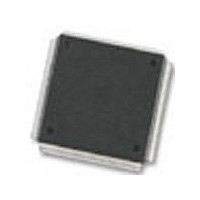
MC68376BAMFT20 Freescale Semiconductor, MC68376BAMFT20 Datasheet - Page 122

MC68376BAMFT20
Manufacturer Part Number
MC68376BAMFT20
Description
Manufacturer
Freescale Semiconductor
Datasheet
1.MC68376BAMFT20.pdf
(434 pages)
Specifications of MC68376BAMFT20
Cpu Family
68K/M683xx
Device Core
ColdFire
Device Core Size
32b
Frequency (max)
20MHz
Interface Type
QSPI/SCI
Program Memory Type
ROM
Program Memory Size
8KB
Total Internal Ram Size
7.5KB
# I/os (max)
18
Number Of Timers - General Purpose
2
Operating Supply Voltage (typ)
5V
Operating Supply Voltage (max)
5.25V
Operating Supply Voltage (min)
4.75V
On-chip Adc
16-chx10-bit
Instruction Set Architecture
RISC
Operating Temp Range
-40C to 125C
Operating Temperature Classification
Automotive
Mounting
Surface Mount
Pin Count
160
Package Type
PQFP
Lead Free Status / Rohs Status
Not Compliant
Available stocks
Company
Part Number
Manufacturer
Quantity
Price
Company:
Part Number:
MC68376BAMFT20
Manufacturer:
FREESCAL
Quantity:
245
- Current page: 122 of 434
- Download datasheet (7Mb)
5.7.3.2 Clock Mode Selection
5-44
MOTOROLA
Data bus mode select current is specified in Table A-5. Do not confuse pin function
with pin electrical state. Refer to 5.7.5 Pin States During Reset for more information.
Unlike other chip-select signals, the boot ROM chip-select (CSBOOT) is active at the
release of RESET. During reset exception processing, the MCU fetches initialization
vectors beginning at address $000000 in supervisor program space. An external
memory device containing vectors located at these addresses can be enabled by
CSBOOT after a reset.
The logic level of DATA0 during reset selects boot ROM port size for dynamic bus al-
location. When DATA0 is held low, port size is eight bits; when DATA0 is held high,
either by the weak internal pull-up driver or by an external pull-up, port size is 16 bits.
Refer to 5.9.4 Chip-Select Reset Operation for more information.
DATA1 and DATA2 determine the functions of CS[2:0] and CS[5:3], respectively.
DATA[7:3] determine the functions of an associated chip-select and all lower-num-
bered chip-selects down through CS6. For example, if DATA5 is pulled low during re-
set, CS[8:6] are assigned alternate function as ADDR[21:19], and CS[10:9] remain
chip-selects. Refer to 5.9.4 Chip-Select Reset Operation for more information.
DATA8 determines the function of the DSACK[1:0], AVEC, DS, AS, and SIZE pins. If
DATA8 is held low during reset, these pins are assigned to I/O port E.
DATA9 determines the function of interrupt request pins IRQ[7:1] and the clock mode
select pin (MODCLK). When DATA9 is held low during reset, these pins are assigned
to I/O port F.
The state of the clock mode (MODCLK) pin during reset determines what clock source
the MCU uses. When MODCLK is held high during reset, the clock signal is generated
from a reference frequency using the clock synthesizer. When MODCLK is held low
during reset, the clock synthesizer is disabled, and an external system clock signal
must be applied. Refer to 5.3 System Clock for more information.
Figure 5-17 Alternate Circuit for Data Bus Mode Select Conditioning
DATA PIN
RESET
1N4148
1 kW
SYSTEM INTEGRATION MODULE
DATA PIN
RESET
2 kW
1 kW
2N3906
USER’S MANUAL
ALTERNATE DATA BUS CONDITION CIRCUIT
MC68336/376
Related parts for MC68376BAMFT20
Image
Part Number
Description
Manufacturer
Datasheet
Request
R
Part Number:
Description:
Manufacturer:
Freescale Semiconductor, Inc
Datasheet:
Part Number:
Description:
Manufacturer:
Freescale Semiconductor, Inc
Datasheet:
Part Number:
Description:
Manufacturer:
Freescale Semiconductor, Inc
Datasheet:
Part Number:
Description:
Manufacturer:
Freescale Semiconductor, Inc
Datasheet:
Part Number:
Description:
Manufacturer:
Freescale Semiconductor, Inc
Datasheet:
Part Number:
Description:
Manufacturer:
Freescale Semiconductor, Inc
Datasheet:
Part Number:
Description:
Manufacturer:
Freescale Semiconductor, Inc
Datasheet:
Part Number:
Description:
Manufacturer:
Freescale Semiconductor, Inc
Datasheet:
Part Number:
Description:
Manufacturer:
Freescale Semiconductor, Inc
Datasheet:
Part Number:
Description:
Manufacturer:
Freescale Semiconductor, Inc
Datasheet:
Part Number:
Description:
Manufacturer:
Freescale Semiconductor, Inc
Datasheet:
Part Number:
Description:
Manufacturer:
Freescale Semiconductor, Inc
Datasheet:
Part Number:
Description:
Manufacturer:
Freescale Semiconductor, Inc
Datasheet:
Part Number:
Description:
Manufacturer:
Freescale Semiconductor, Inc
Datasheet:
Part Number:
Description:
Manufacturer:
Freescale Semiconductor, Inc
Datasheet:


