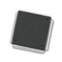
MC68376BAMFT20 Freescale Semiconductor, MC68376BAMFT20 Datasheet - Page 184

MC68376BAMFT20
Manufacturer Part Number
MC68376BAMFT20
Description
Manufacturer
Freescale Semiconductor
Datasheet
1.MC68376BAMFT20.pdf
(434 pages)
Specifications of MC68376BAMFT20
Cpu Family
68K/M683xx
Device Core
ColdFire
Device Core Size
32b
Frequency (max)
20MHz
Interface Type
QSPI/SCI
Program Memory Type
ROM
Program Memory Size
8KB
Total Internal Ram Size
7.5KB
# I/os (max)
18
Number Of Timers - General Purpose
2
Operating Supply Voltage (typ)
5V
Operating Supply Voltage (max)
5.25V
Operating Supply Voltage (min)
4.75V
On-chip Adc
16-chx10-bit
Instruction Set Architecture
RISC
Operating Temp Range
-40C to 125C
Operating Temperature Classification
Automotive
Mounting
Surface Mount
Pin Count
160
Package Type
PQFP
Lead Free Status / Rohs Status
Not Compliant
Available stocks
Company
Part Number
Manufacturer
Quantity
Price
Company:
Part Number:
MC68376BAMFT20
Manufacturer:
FREESCAL
Quantity:
245
- Current page: 184 of 434
- Download datasheet (7Mb)
8.2 QADC Address Map
8.3 QADC Registers
8.4 QADC Pin Functions
8-2
MOTOROLA
The QADC occupies 512 bytes of address space. Nine words are control, port, and
status registers, 40 words are the CCW table, and 120 words are the result word table
because 40 result registers can be read in three data alignment formats. The remain-
ing words are reserved for expansion. Refer to D.5 QADC Module for information con-
cerning the QADC address map.
The QADC has three global registers for configuring module operation: the module
configuration register (QADCMCR), the interrupt register (QADCINT), and a test reg-
ister (QADCTEST). The global registers are always defined to be in supervisor data
space. The CPU32 allows software to establish the global registers in supervisor data
space and the remaining registers and tables in user space.
All QADC analog channel/port pins that are not used for analog input channels can be
used as digital port pins. Port values are read/written by accessing the port A and B
data registers (PORTQA and PORTQB). Port A pins are specified as inputs or outputs
by programming the port data direction register (DDRQA). Port B is an input only port.
The four remaining control registers configure the operation of the queuing mecha-
nism, and provide a means of monitoring the operation of the QADC. Control register
0 (QACR0) contains hardware configuration information. Control register 1 (QACR1)
is associated with queue 1, and control register 2 (QACR2) is associated with queue
2. The status register (QASR) provides visibility on the status of each queue and the
particular conversion that is in progress.
Following the register block in the address map is the CCW table. There are 40 words
to hold the desired analog conversion sequences. Each CCW is a 16-bit word, with ten
implemented bits in four fields. Refer to D.5.8 Conversion Command Word Table for
more information.
The final block of address space belongs to the result word table, which appears in
three places in the memory map. Each result word table location holds one 10-bit con-
version value. The software selects one of three data formats, which map the 10-bit
result onto the 16-bit data bus by reading the address which produces the desired
alignment. The first address block presents the result data in right justified format, the
second block is presented in left justified signed format, and the third is presented in
left justified unsigned format. Refer to D.5.9 Result Word Table for more information.
The QADC uses a maximum of 21 external pins. There are 16 channel/port pins that
can support up to 41 channels when external multiplexing is used (including internal
channels). All of the channel pins can also be used as general-purpose digital port
pins.
In addition, there are also two analog reference pins, two analog submodule power
pins, and one V
SS
QUEUED ANALOG-TO-DIGITAL CONVERTER MODULE
pin for the open drain output drivers on port A.
USER’S MANUAL
MC68336/376
Related parts for MC68376BAMFT20
Image
Part Number
Description
Manufacturer
Datasheet
Request
R
Part Number:
Description:
Manufacturer:
Freescale Semiconductor, Inc
Datasheet:
Part Number:
Description:
Manufacturer:
Freescale Semiconductor, Inc
Datasheet:
Part Number:
Description:
Manufacturer:
Freescale Semiconductor, Inc
Datasheet:
Part Number:
Description:
Manufacturer:
Freescale Semiconductor, Inc
Datasheet:
Part Number:
Description:
Manufacturer:
Freescale Semiconductor, Inc
Datasheet:
Part Number:
Description:
Manufacturer:
Freescale Semiconductor, Inc
Datasheet:
Part Number:
Description:
Manufacturer:
Freescale Semiconductor, Inc
Datasheet:
Part Number:
Description:
Manufacturer:
Freescale Semiconductor, Inc
Datasheet:
Part Number:
Description:
Manufacturer:
Freescale Semiconductor, Inc
Datasheet:
Part Number:
Description:
Manufacturer:
Freescale Semiconductor, Inc
Datasheet:
Part Number:
Description:
Manufacturer:
Freescale Semiconductor, Inc
Datasheet:
Part Number:
Description:
Manufacturer:
Freescale Semiconductor, Inc
Datasheet:
Part Number:
Description:
Manufacturer:
Freescale Semiconductor, Inc
Datasheet:
Part Number:
Description:
Manufacturer:
Freescale Semiconductor, Inc
Datasheet:
Part Number:
Description:
Manufacturer:
Freescale Semiconductor, Inc
Datasheet:


