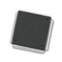
MC68376BAMFT20 Freescale Semiconductor, MC68376BAMFT20 Datasheet - Page 156

MC68376BAMFT20
Manufacturer Part Number
MC68376BAMFT20
Description
Manufacturer
Freescale Semiconductor
Datasheet
1.MC68376BAMFT20.pdf
(434 pages)
Specifications of MC68376BAMFT20
Cpu Family
68K/M683xx
Device Core
ColdFire
Device Core Size
32b
Frequency (max)
20MHz
Interface Type
QSPI/SCI
Program Memory Type
ROM
Program Memory Size
8KB
Total Internal Ram Size
7.5KB
# I/os (max)
18
Number Of Timers - General Purpose
2
Operating Supply Voltage (typ)
5V
Operating Supply Voltage (max)
5.25V
Operating Supply Voltage (min)
4.75V
On-chip Adc
16-chx10-bit
Instruction Set Architecture
RISC
Operating Temp Range
-40C to 125C
Operating Temperature Classification
Automotive
Mounting
Surface Mount
Pin Count
160
Package Type
PQFP
Lead Free Status / Rohs Status
Not Compliant
Available stocks
Company
Part Number
Manufacturer
Quantity
Price
Company:
Part Number:
MC68376BAMFT20
Manufacturer:
FREESCAL
Quantity:
245
- Current page: 156 of 434
- Download datasheet (7Mb)
9.3.1 QSPI Registers
9.3.1.1 Control Registers
9-6
MOTOROLA
Serial transfers of eight to sixteen can be specified. Programmable transfer length sim-
plifies interfacing to devices that require different data lengths.
An inter-transfer delay of 17 to 8192 system clocks can be specified (default is 17 sys-
tem clocks). Programmable delay simplifies the interface to devices that require differ-
ent delays between transfers.
A dedicated 80-byte RAM is used to store received data, data to be transmitted, and
a queue of commands. The CPU32 can access these locations directly. This allows
serial peripherals to be treated like memory-mapped parallel devices.
The command queue allows the QSPI to perform up to 16 serial transfers without
CPU32 intervention. Each queue entry contains all the information needed by the
QSPI to independently complete one serial transfer.
A pointer identifies the queue location containing the data and command for the next
serial transfer. Normally, the pointer address is incremented after each serial transfer,
but the CPU32 can change the pointer value at any time. Support of multiple-tasks can
be provided by segmenting the queue.
The QSPI has four peripheral chip-select pins. The chip-select signals simplify inter-
facing by reducing CPU32 intervention. If the chip-select signals are externally decod-
ed, 16 independent select signals can be generated.
Wrap-around mode allows continuous execution of queued commands. In wrap-
around mode, newly received data replaces previously received data in the receive
RAM. Wrap-around mode can simplify the interface with A/D converters by continu-
ously updating conversion values stored in the RAM.
Continuous transfer mode allows transfer of an uninterrupted bit stream. Any number
of bits in a range from 8 to 256 can be transferred without CPU32 intervention. Longer
transfers are possible, but minimal intervention is required to prevent loss of data. A
standard delay of 17 system clocks is inserted between the transfer of each queue
entry.
The programmer’s model for the QSPI consists of the QSM global and pin control reg-
isters, four QSPI control registers (SPCR[0:3]), the status register (SPSR), and the 80-
byte QSPI RAM. Registers and RAM can be read and written by the CPU32. Refer to
D.6 Queued Serial Module for register bit and field definitions.
Control registers contain parameters for configuring the QSPI and enabling various
modes of operation. The CPU32 has read and write access to all control registers. The
QSM has read access only to all bits except the SPE bit in SPCR1. Control registers
must be initialized before the QSPI is enabled to insure defined operation. SPCR1
must be written last because it contains the QSPI enable bit (SPE).
Writing a new value to any control register except SPCR2 while the QSPI is enabled
disrupts operation. SPCR2 is buffered. New SPCR2 values become effective after
completion of the current serial transfer. Rewriting NEWQP in SPCR2 causes execu-
QUEUED SERIAL MODULE
USER’S MANUAL
MC68336/376
Related parts for MC68376BAMFT20
Image
Part Number
Description
Manufacturer
Datasheet
Request
R
Part Number:
Description:
Manufacturer:
Freescale Semiconductor, Inc
Datasheet:
Part Number:
Description:
Manufacturer:
Freescale Semiconductor, Inc
Datasheet:
Part Number:
Description:
Manufacturer:
Freescale Semiconductor, Inc
Datasheet:
Part Number:
Description:
Manufacturer:
Freescale Semiconductor, Inc
Datasheet:
Part Number:
Description:
Manufacturer:
Freescale Semiconductor, Inc
Datasheet:
Part Number:
Description:
Manufacturer:
Freescale Semiconductor, Inc
Datasheet:
Part Number:
Description:
Manufacturer:
Freescale Semiconductor, Inc
Datasheet:
Part Number:
Description:
Manufacturer:
Freescale Semiconductor, Inc
Datasheet:
Part Number:
Description:
Manufacturer:
Freescale Semiconductor, Inc
Datasheet:
Part Number:
Description:
Manufacturer:
Freescale Semiconductor, Inc
Datasheet:
Part Number:
Description:
Manufacturer:
Freescale Semiconductor, Inc
Datasheet:
Part Number:
Description:
Manufacturer:
Freescale Semiconductor, Inc
Datasheet:
Part Number:
Description:
Manufacturer:
Freescale Semiconductor, Inc
Datasheet:
Part Number:
Description:
Manufacturer:
Freescale Semiconductor, Inc
Datasheet:
Part Number:
Description:
Manufacturer:
Freescale Semiconductor, Inc
Datasheet:


