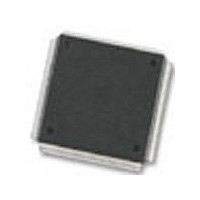
MC68376BAMFT20 Freescale Semiconductor, MC68376BAMFT20 Datasheet - Page 187

MC68376BAMFT20
Manufacturer Part Number
MC68376BAMFT20
Description
Manufacturer
Freescale Semiconductor
Datasheet
1.MC68376BAMFT20.pdf
(434 pages)
Specifications of MC68376BAMFT20
Cpu Family
68K/M683xx
Device Core
ColdFire
Device Core Size
32b
Frequency (max)
20MHz
Interface Type
QSPI/SCI
Program Memory Type
ROM
Program Memory Size
8KB
Total Internal Ram Size
7.5KB
# I/os (max)
18
Number Of Timers - General Purpose
2
Operating Supply Voltage (typ)
5V
Operating Supply Voltage (max)
5.25V
Operating Supply Voltage (min)
4.75V
On-chip Adc
16-chx10-bit
Instruction Set Architecture
RISC
Operating Temp Range
-40C to 125C
Operating Temperature Classification
Automotive
Mounting
Surface Mount
Pin Count
160
Package Type
PQFP
Lead Free Status / Rohs Status
Not Compliant
Available stocks
Company
Part Number
Manufacturer
Quantity
Price
Company:
Part Number:
MC68376BAMFT20
Manufacturer:
FREESCAL
Quantity:
245
- Current page: 187 of 434
- Download datasheet (7Mb)
8.4.3 External Trigger Input Pins
8.4.4 Multiplexed Address Output Pins
8.4.5 Multiplexed Analog Input Pins
8.4.6 Voltage Reference Pins
MC68336/376
USER’S MANUAL
The QADC has two external trigger pins (ETRIG[2:1]). The external trigger pins share
two multifunction port A pins (PQA[4:3]), which are normally used as analog channel
input pins. Each of the two external trigger pins is associated with one of the scan
queues. When a queue is in external trigger mode, the corresponding external trigger
pin is configured as a digital input and the software programmed input/output direction
for that pin is ignored. Refer to D.5.5 Port Data Direction Register for more informa-
tion.
In non-multiplexed mode, the 16 channel pins are connected to an internal multiplexer
which routes the analog signals into the A/D converter.
In externally multiplexed mode, the QADC allows automatic channel selection through
up to four external 1-of-8 multiplexer chips. The QADC provides a 3-bit multiplexed ad-
dress output to the external mux chips to allow selection of one of eight inputs. The
multiplexed address output signals MA[2:0] can be used as multiplex address output
bits or as general-purpose I/O.
MA[2:0] are used as the address inputs for up to four 1-of-8 multiplexer chips (for ex-
ample, the MC14051 and the MC74HC4051). Since MA[2:0] are digital outputs in mul-
tiplexed mode, the software programmed input/output direction for these pins in
DDRQA is ignored.
In externally multiplexed mode, four of the port B pins are redefined to each represent
a group of eight input channels. Refer to Table 8-1.
The analog output of each external multiplexer chip is connected to one of the AN[w,
x, y, z] inputs in order to convert a channel selected by the MA[2:0] multiplexed ad-
dress outputs.
V
arating the reference inputs from the power supply pins allows for additional external
filtering, which increases reference voltage precision and stability, and subsequently
contributes to a higher degree of conversion accuracy. Refer to Tables A-11 and A-
12 for more information.
RH
and V
RL
are the dedicated input pins for the high and low reference voltages. Sep-
Multiplexed Analog Input
QUEUED ANALOG-TO-DIGITAL CONVERTER MODULE
Table 8-1 Multiplexed Analog Input Channels
ANw
ANx
ANy
ANz
Even numbered channels from 0 to 14
Odd numbered channels from 1 to 15
Even channels from 16 to 30
Odd channels from 17 to 31
Channels
MOTOROLA
8-5
Related parts for MC68376BAMFT20
Image
Part Number
Description
Manufacturer
Datasheet
Request
R
Part Number:
Description:
Manufacturer:
Freescale Semiconductor, Inc
Datasheet:
Part Number:
Description:
Manufacturer:
Freescale Semiconductor, Inc
Datasheet:
Part Number:
Description:
Manufacturer:
Freescale Semiconductor, Inc
Datasheet:
Part Number:
Description:
Manufacturer:
Freescale Semiconductor, Inc
Datasheet:
Part Number:
Description:
Manufacturer:
Freescale Semiconductor, Inc
Datasheet:
Part Number:
Description:
Manufacturer:
Freescale Semiconductor, Inc
Datasheet:
Part Number:
Description:
Manufacturer:
Freescale Semiconductor, Inc
Datasheet:
Part Number:
Description:
Manufacturer:
Freescale Semiconductor, Inc
Datasheet:
Part Number:
Description:
Manufacturer:
Freescale Semiconductor, Inc
Datasheet:
Part Number:
Description:
Manufacturer:
Freescale Semiconductor, Inc
Datasheet:
Part Number:
Description:
Manufacturer:
Freescale Semiconductor, Inc
Datasheet:
Part Number:
Description:
Manufacturer:
Freescale Semiconductor, Inc
Datasheet:
Part Number:
Description:
Manufacturer:
Freescale Semiconductor, Inc
Datasheet:
Part Number:
Description:
Manufacturer:
Freescale Semiconductor, Inc
Datasheet:
Part Number:
Description:
Manufacturer:
Freescale Semiconductor, Inc
Datasheet:


