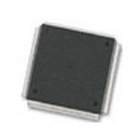
MC68376BAMFT20 Freescale Semiconductor, MC68376BAMFT20 Datasheet - Page 154

MC68376BAMFT20
Manufacturer Part Number
MC68376BAMFT20
Description
Manufacturer
Freescale Semiconductor
Datasheet
1.MC68376BAMFT20.pdf
(434 pages)
Specifications of MC68376BAMFT20
Cpu Family
68K/M683xx
Device Core
ColdFire
Device Core Size
32b
Frequency (max)
20MHz
Interface Type
QSPI/SCI
Program Memory Type
ROM
Program Memory Size
8KB
Total Internal Ram Size
7.5KB
# I/os (max)
18
Number Of Timers - General Purpose
2
Operating Supply Voltage (typ)
5V
Operating Supply Voltage (max)
5.25V
Operating Supply Voltage (min)
4.75V
On-chip Adc
16-chx10-bit
Instruction Set Architecture
RISC
Operating Temp Range
-40C to 125C
Operating Temperature Classification
Automotive
Mounting
Surface Mount
Pin Count
160
Package Type
PQFP
Lead Free Status / Rohs Status
Not Compliant
Available stocks
Company
Part Number
Manufacturer
Quantity
Price
Company:
Part Number:
MC68376BAMFT20
Manufacturer:
FREESCAL
Quantity:
245
- Current page: 154 of 434
- Download datasheet (7Mb)
9.2.2 QSM Pin Control Registers
9-4
MOTOROLA
The QSM uses nine pins. Eight of the pins can be used for serial communication or for
parallel I/O. Clearing a bit in the port QS pin assignment register (PQSPAR) assigns
the corresponding pin to general-purpose I/O; setting a bit assigns the pin to the QSPI.
PQSPAR does not select I/O. In master mode, PQSPAR causes a bit to be assigned
to the QSPI when SPE is set. In slave mode, the MISO pin, if assigned to the QSPI,
remains under the control of the QSPI, regardless of the SPE bit. PQSPAR does not
affect operation of the SCI.
The port QS data direction register (DDRQS) determines whether pins are inputs or
outputs. Clearing a bit makes the corresponding pin an input; setting a bit makes the
pin an output. DDRQS affects both QSPI function and I/O function. DDQS7 deter-
mines the direction of the TXD pin only when the SCI transmitter is disabled. When the
SCI transmitter is enabled, the TXD pin is an output. PQSPAR and DDRQS are 8-bit
registers located at the same word address. Table 9-1 is a summary of QSM pin func-
tions.
The port QS data register (PORTQS) latches I/O data. PORTQS writes drive pins de-
fined as outputs. PORTQS reads return data present on the pins. To avoid driving un-
defined data, first write PORTQS, then configure DDRQS.
NOTES:
PCS0/SS
QSM Pin
PCS[1:3]
MISO
MOSI
SCK
TXD
1. PQS2 is a digital I/O pin unless the SPI is enabled (SPE set in SPCR1), in which case it
2. PQS7 is a digital I/O pin unless the SCI transmitter is enabled (TE set in SCCR1), in
RXD
becomes the QSPI serial clock SCK.
which case it becomes the SCI serial data output TXD.
1
2
Table 9-1 Effect of DDRQS on QSM Pin Function
Master
Master
Master
Master
Master
Mode
Slave
Slave
Slave
Slave
Slave
—
—
DDRQS Bit
DDQS[4:6]
QUEUED SERIAL MODULE
DDQS0
DDQS1
DDQS2
DDQS3
DDQS7
None
Bit State
NA
—
—
X
0
1
0
1
0
1
0
1
0
1
0
1
0
1
0
1
Serial data output from QSPI
Serial data output from QSPI
Assertion causes mode fault
Serial data output from SCI
Disables chip-select output
Disables slave select input
Serial data input to QSPI
Serial data input to QSPI
Clock output from QSPI
QSPI slave select input
Serial data input to SCI
Disables data output
Disables data output
Clock input to QSPI
Disables data input
Disables data input
Chip-select output
Chip-select output
Pin Function
Inactive
Inactive
USER’S MANUAL
MC68336/376
Related parts for MC68376BAMFT20
Image
Part Number
Description
Manufacturer
Datasheet
Request
R
Part Number:
Description:
Manufacturer:
Freescale Semiconductor, Inc
Datasheet:
Part Number:
Description:
Manufacturer:
Freescale Semiconductor, Inc
Datasheet:
Part Number:
Description:
Manufacturer:
Freescale Semiconductor, Inc
Datasheet:
Part Number:
Description:
Manufacturer:
Freescale Semiconductor, Inc
Datasheet:
Part Number:
Description:
Manufacturer:
Freescale Semiconductor, Inc
Datasheet:
Part Number:
Description:
Manufacturer:
Freescale Semiconductor, Inc
Datasheet:
Part Number:
Description:
Manufacturer:
Freescale Semiconductor, Inc
Datasheet:
Part Number:
Description:
Manufacturer:
Freescale Semiconductor, Inc
Datasheet:
Part Number:
Description:
Manufacturer:
Freescale Semiconductor, Inc
Datasheet:
Part Number:
Description:
Manufacturer:
Freescale Semiconductor, Inc
Datasheet:
Part Number:
Description:
Manufacturer:
Freescale Semiconductor, Inc
Datasheet:
Part Number:
Description:
Manufacturer:
Freescale Semiconductor, Inc
Datasheet:
Part Number:
Description:
Manufacturer:
Freescale Semiconductor, Inc
Datasheet:
Part Number:
Description:
Manufacturer:
Freescale Semiconductor, Inc
Datasheet:
Part Number:
Description:
Manufacturer:
Freescale Semiconductor, Inc
Datasheet:


