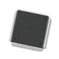
MC68376BAMFT20 Freescale Semiconductor, MC68376BAMFT20 Datasheet - Page 253

MC68376BAMFT20
Manufacturer Part Number
MC68376BAMFT20
Description
Manufacturer
Freescale Semiconductor
Datasheet
1.MC68376BAMFT20.pdf
(434 pages)
Specifications of MC68376BAMFT20
Cpu Family
68K/M683xx
Device Core
ColdFire
Device Core Size
32b
Frequency (max)
20MHz
Interface Type
QSPI/SCI
Program Memory Type
ROM
Program Memory Size
8KB
Total Internal Ram Size
7.5KB
# I/os (max)
18
Number Of Timers - General Purpose
2
Operating Supply Voltage (typ)
5V
Operating Supply Voltage (max)
5.25V
Operating Supply Voltage (min)
4.75V
On-chip Adc
16-chx10-bit
Instruction Set Architecture
RISC
Operating Temp Range
-40C to 125C
Operating Temperature Classification
Automotive
Mounting
Surface Mount
Pin Count
160
Package Type
PQFP
Lead Free Status / Rohs Status
Not Compliant
Available stocks
Company
Part Number
Manufacturer
Quantity
Price
Company:
Part Number:
MC68376BAMFT20
Manufacturer:
FREESCAL
Quantity:
245
- Current page: 253 of 434
- Download datasheet (7Mb)
12.1 General
12.2 TPURAM Register Block
12.3 TPURAM Array Address Mapping
MC68336/376
USER’S MANUAL
The standby RAM module with TPU emulation capability (TPURAM) consists of a
control register block and a 3.5-Kbyte array of fast (two system clock) static RAM,
which is especially useful for system stacks and variable storage. The TPURAM re-
sponds to both program and data space accesses. The TPURAM can also be used to
emulate TPU microcode ROM.
The TPURAM can be mapped to the lower 3.5 Kbytes of any 4-Kbyte boundary in the
address map, but must not overlap the module control registers as overlap makes the
registers inaccessible. Data can be read or written in bytes, words or long words. The
TPURAM is powered by V
tents can be maintained by power from the V
sources is automatic.
There are three TPURAM control registers: the TPURAM module configuration regis-
ter (TRAMMCR), the TPURAM test register (TRAMTST), and the TPURAM base ad-
dress and status register (TRAMBAR). To protect these registers from accidental
modification, they are always mapped to supervisor data space.
The TPURAM control register block begins at address $7FFB00 or $FFFB00, depend-
ing on the value of the module mapping (MM) bit in the SIM configuration register
(SIMCR). Refer to 5.2.1 Module Mapping for more information on how the state of
MM affects the system.
The TPURAM control register block occupies eight bytes of address space. Unimple-
mented register addresses are read as zeros, and writes have no effect. Refer to D.9
Standby RAM Module with TPU Emulation Capability (TPURAM) for register block
address map and register bit/field definitions.
The base address and status register TRAMBAR specifies the TPURAM array base
address in the MCU memory map. TRAMBAR[15:4] specify the 12 high-order bits of
the base address. The TPU bus interface unit compares these bits to address lines
ADDR[23:12]. If the two match, then the low order address lines and the SIZ[1:0] sig-
nals are used to access the RAM location in the array.
The RAM disable (RAMDS) bit, the LSB of TRAMBAR, indicates whether the
TPURAM array is active (RAMDS = 0) or disabled (RAMDS = 1). The array is disabled
coming out of reset and remains disabled if the base address field is programmed with
an address that overlaps the address of the module control register block. Writing a
valid base address to TRAMBAR[15:4] clears RAMDS and enables the array.
SECTION 12 STANDBY RAM WITH TPU EMULATION
STANDBY RAM WITH TPU EMULATION
DD
in normal operation. During power-down, TPURAM con-
STBY
input. Power switching between
MOTOROLA
12-1
Related parts for MC68376BAMFT20
Image
Part Number
Description
Manufacturer
Datasheet
Request
R
Part Number:
Description:
Manufacturer:
Freescale Semiconductor, Inc
Datasheet:
Part Number:
Description:
Manufacturer:
Freescale Semiconductor, Inc
Datasheet:
Part Number:
Description:
Manufacturer:
Freescale Semiconductor, Inc
Datasheet:
Part Number:
Description:
Manufacturer:
Freescale Semiconductor, Inc
Datasheet:
Part Number:
Description:
Manufacturer:
Freescale Semiconductor, Inc
Datasheet:
Part Number:
Description:
Manufacturer:
Freescale Semiconductor, Inc
Datasheet:
Part Number:
Description:
Manufacturer:
Freescale Semiconductor, Inc
Datasheet:
Part Number:
Description:
Manufacturer:
Freescale Semiconductor, Inc
Datasheet:
Part Number:
Description:
Manufacturer:
Freescale Semiconductor, Inc
Datasheet:
Part Number:
Description:
Manufacturer:
Freescale Semiconductor, Inc
Datasheet:
Part Number:
Description:
Manufacturer:
Freescale Semiconductor, Inc
Datasheet:
Part Number:
Description:
Manufacturer:
Freescale Semiconductor, Inc
Datasheet:
Part Number:
Description:
Manufacturer:
Freescale Semiconductor, Inc
Datasheet:
Part Number:
Description:
Manufacturer:
Freescale Semiconductor, Inc
Datasheet:
Part Number:
Description:
Manufacturer:
Freescale Semiconductor, Inc
Datasheet:


