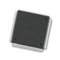
MC68376BAMFT20 Freescale Semiconductor, MC68376BAMFT20 Datasheet - Page 137

MC68376BAMFT20
Manufacturer Part Number
MC68376BAMFT20
Description
Manufacturer
Freescale Semiconductor
Datasheet
1.MC68376BAMFT20.pdf
(434 pages)
Specifications of MC68376BAMFT20
Cpu Family
68K/M683xx
Device Core
ColdFire
Device Core Size
32b
Frequency (max)
20MHz
Interface Type
QSPI/SCI
Program Memory Type
ROM
Program Memory Size
8KB
Total Internal Ram Size
7.5KB
# I/os (max)
18
Number Of Timers - General Purpose
2
Operating Supply Voltage (typ)
5V
Operating Supply Voltage (max)
5.25V
Operating Supply Voltage (min)
4.75V
On-chip Adc
16-chx10-bit
Instruction Set Architecture
RISC
Operating Temp Range
-40C to 125C
Operating Temperature Classification
Automotive
Mounting
Surface Mount
Pin Count
160
Package Type
PQFP
Lead Free Status / Rohs Status
Not Compliant
Available stocks
Company
Part Number
Manufacturer
Quantity
Price
Company:
Part Number:
MC68376BAMFT20
Manufacturer:
FREESCAL
Quantity:
245
- Current page: 137 of 434
- Download datasheet (7Mb)
5.9.1.3 Chip-Select Option Registers
MC68336/376
USER’S MANUAL
The chip-select address compare logic uses only the most significant bits to match an
address within a block. The value of the base address must be an integer multiple of
the block size.
After reset, the MCU fetches the initialization routine from the address contained in the
reset vector, located beginning at address $000000 of program space. To support
bootstrap operation from reset, the base address field in the boot chip-select base ad-
dress register (CSBARBT) has a reset value of $000, which corresponds to a base ad-
dress of $000000 and a block size of one Mbyte. A memory device containing the reset
vector and initialization routine can be automatically enabled by CSBOOT after a re-
set. Refer to 5.9.4 Chip-Select Reset Operation for more information.
Option register fields determine timing of and conditions for assertion of chip-select
signals. To assert a chip-select signal, and to provide DSACK or autovector support,
other constraints set by fields in the option register and in the base address register
must also be satisfied. The following paragraphs summarize option register functions.
Refer to D.2.21 Chip-Select Option Registers for register and bit field information.
The MODE bit determines whether chip-select assertion simulates an asynchronous
bus cycle, or is synchronized to the M6800-type bus clock signal ECLK available on
ADDR23. Refer to 5.3 System Clock for more information on ECLK.
BYTE[1:0] controls bus allocation for chip-select transfers. Port size, set when a chip-
select is enabled by a pin assignment register, affects signal assertion. When an 8-bit
port is assigned, any BYTE field value other than %00 enables the chip-select signal.
When a 16-bit port is assigned, however, BYTE field value determines when the chip-
select is enabled. The BYTE fields for CS[10:0] are cleared during reset. However,
both bits in the boot ROM chip-select option register (CSORBT) BYTE field are set
(%11) when the RESET signal is released.
R/W[1:0] causes a chip-select signal to be asserted only for a read, only for a write, or
for both read and write. Use this field in conjunction with the STRB bit to generate
asynchronous control signals for external devices.
BLKSZ[2:0]
000
001
010
011
100
101
110
111
Table 5-20 Block Size Encoding
SYSTEM INTEGRATION MODULE
Block Size
128 Kbytes
256 Kbytes
512 Kbytes
16 Kbytes
64 Kbytes
2 Kbytes
8 Kbytes
1 Mbyte
Address Lines Compared
ADDR[23:11]
ADDR[23:13]
ADDR[23:14]
ADDR[23:16]
ADDR[23:17]
ADDR[23:18]
ADDR[23:19]
ADDR[23:20]
MOTOROLA
5-59
Related parts for MC68376BAMFT20
Image
Part Number
Description
Manufacturer
Datasheet
Request
R
Part Number:
Description:
Manufacturer:
Freescale Semiconductor, Inc
Datasheet:
Part Number:
Description:
Manufacturer:
Freescale Semiconductor, Inc
Datasheet:
Part Number:
Description:
Manufacturer:
Freescale Semiconductor, Inc
Datasheet:
Part Number:
Description:
Manufacturer:
Freescale Semiconductor, Inc
Datasheet:
Part Number:
Description:
Manufacturer:
Freescale Semiconductor, Inc
Datasheet:
Part Number:
Description:
Manufacturer:
Freescale Semiconductor, Inc
Datasheet:
Part Number:
Description:
Manufacturer:
Freescale Semiconductor, Inc
Datasheet:
Part Number:
Description:
Manufacturer:
Freescale Semiconductor, Inc
Datasheet:
Part Number:
Description:
Manufacturer:
Freescale Semiconductor, Inc
Datasheet:
Part Number:
Description:
Manufacturer:
Freescale Semiconductor, Inc
Datasheet:
Part Number:
Description:
Manufacturer:
Freescale Semiconductor, Inc
Datasheet:
Part Number:
Description:
Manufacturer:
Freescale Semiconductor, Inc
Datasheet:
Part Number:
Description:
Manufacturer:
Freescale Semiconductor, Inc
Datasheet:
Part Number:
Description:
Manufacturer:
Freescale Semiconductor, Inc
Datasheet:
Part Number:
Description:
Manufacturer:
Freescale Semiconductor, Inc
Datasheet:


