R0K561622S000BE Renesas Electronics America, R0K561622S000BE Datasheet - Page 824
R0K561622S000BE
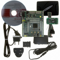
Manufacturer Part Number
R0K561622S000BE
Description
KIT STARTER FOR H8SX/1622
Manufacturer
Renesas Electronics America
Series
Renesas Starter Kits (RSK)r
Type
MCUr
Specifications of R0K561622S000BE
Contents
Board, Cables, CD, Debugger, Power Supply
Silicon Manufacturer
Renesas
Features
Coding And Debugging, E10A Emulator, RS232 Serial Connection
Kit Contents
Board
Silicon Family Name
H8SX/1622F
Silicon Core Number
R5F61622N50LGV
Lead Free Status / RoHS Status
Lead free / RoHS Compliant
For Use With/related Products
H8SX/1622
Lead Free Status / RoHS Status
Lead free / RoHS Compliant, Lead free / RoHS Compliant


Section 22 Flash Memory
Initialization before Programming/Erasure: The on-chip program includes the initialization
program. A pulse with the specified period must be applied when programming or erasing. The
specified pulse width is made by the method in which wait loop is configured by the CPU
instruction. Accordingly, the operating frequency of the CPU must be set. The initial program is
set as a parameter of the programming/erasing program which has been downloaded to perform
these settings.
Programming: When the flash memory is programmed, the start address of the programming
destination on the user MAT and the program data must be passed to the programming program.
The start address of the programming destination on the user MAT must be stored in general
register ER1. This parameter is called the flash multipurpose address area parameter (FMPAR).
The program data is always in 128-byte units. When the program data does not satisfy 128 bytes,
128-byte program data is prepared by filling the dummy code (H'FF). The boundary of the start
address of the programming destination on the user MAT is aligned at an address where the lower
eight bits (A7 to A0) are H'00 or H'80.
The program data for the user MAT must be prepared in consecutive areas. The program data
must be in a consecutive space which can be accessed using the MOV.B instruction of the CPU
and is not in the flash memory space.
The start address of the area that stores the data to be written in the user MAT must be set in
general register ER0. This parameter is called the flash multipurpose data destination area
parameter (FMPDR).
For details on the programming procedure, see section 22.8.2, User Program Mode.
Erasure: When the flash memory is erased, the erase block number on the user MAT must be
passed to the erasing program which is downloaded.
The erase block number on the user MAT must be set in general register ER0. This parameter is
called the flash erase block select parameter (FEBS).
One block is selected from the block numbers of 0 to 11 as the erase block number.
For details on the erasing procedure, see section 22.8.2, User Program Mode.
Rev. 2.00 Sep. 16, 2009 Page 794 of 1036
REJ09B0414-0200
Related parts for R0K561622S000BE
Image
Part Number
Description
Manufacturer
Datasheet
Request
R

Part Number:
Description:
KIT STARTER FOR M16C/29
Manufacturer:
Renesas Electronics America
Datasheet:

Part Number:
Description:
KIT STARTER FOR R8C/2D
Manufacturer:
Renesas Electronics America
Datasheet:

Part Number:
Description:
R0K33062P STARTER KIT
Manufacturer:
Renesas Electronics America
Datasheet:

Part Number:
Description:
KIT STARTER FOR R8C/23 E8A
Manufacturer:
Renesas Electronics America
Datasheet:

Part Number:
Description:
KIT STARTER FOR R8C/25
Manufacturer:
Renesas Electronics America
Datasheet:

Part Number:
Description:
KIT STARTER H8S2456 SHARPE DSPLY
Manufacturer:
Renesas Electronics America
Datasheet:

Part Number:
Description:
KIT STARTER FOR R8C38C
Manufacturer:
Renesas Electronics America
Datasheet:

Part Number:
Description:
KIT STARTER FOR R8C35C
Manufacturer:
Renesas Electronics America
Datasheet:

Part Number:
Description:
KIT STARTER FOR R8CL3AC+LCD APPS
Manufacturer:
Renesas Electronics America
Datasheet:
Part Number:
Description:
KIT STARTER FOR RX610
Manufacturer:
Renesas Electronics America
Datasheet:

Part Number:
Description:
KIT STARTER FOR R32C/118
Manufacturer:
Renesas Electronics America
Datasheet:

Part Number:
Description:
KIT DEV RSK-R8C/26-29
Manufacturer:
Renesas Electronics America
Datasheet:

Part Number:
Description:
KIT STARTER FOR SH7124
Manufacturer:
Renesas Electronics America
Datasheet:

Part Number:
Description:
KIT DEV FOR SH7203
Manufacturer:
Renesas Electronics America
Datasheet:
Part Number:
Description:
KIT STARTER FOR R8C/18191A1B
Manufacturer:
Renesas Electronics America
Datasheet: