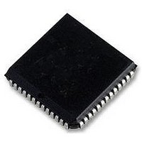
MC68HC11E0CFNE3 Freescale Semiconductor, MC68HC11E0CFNE3 Datasheet - Page 96

MC68HC11E0CFNE3
Manufacturer Part Number
MC68HC11E0CFNE3
Description
IC MCU 8BIT 3MHZ 52-PLCC
Manufacturer
Freescale Semiconductor
Series
HC11r
Specifications of MC68HC11E0CFNE3
Core Processor
HC11
Core Size
8-Bit
Speed
3MHz
Connectivity
SCI, SPI
Peripherals
POR, WDT
Number Of I /o
38
Program Memory Type
ROMless
Ram Size
512 x 8
Voltage - Supply (vcc/vdd)
4.5 V ~ 5.5 V
Data Converters
A/D 8x8b
Oscillator Type
Internal
Operating Temperature
-40°C ~ 85°C
Package / Case
52-PLCC
Controller Family/series
68HC11
No. Of I/o's
38
Ram Memory Size
512Byte
Cpu Speed
3MHz
No. Of Timers
1
Embedded Interface Type
SCI, SPI
Digital Ic Case Style
LCC
Rohs Compliant
Yes
Processor Series
HC11E
Core
HC11
Data Bus Width
8 bit
Data Ram Size
512 B
Interface Type
SCI, SPI
Maximum Clock Frequency
3 MHz
Number Of Programmable I/os
38
Number Of Timers
8
Maximum Operating Temperature
+ 85 C
Mounting Style
SMD/SMT
Minimum Operating Temperature
- 40 C
On-chip Adc
8 bit, 8 Channel
Lead Free Status / RoHS Status
Lead free / RoHS Compliant
Eeprom Size
-
Program Memory Size
-
Lead Free Status / Rohs Status
Details
Available stocks
Company
Part Number
Manufacturer
Quantity
Price
Company:
Part Number:
MC68HC11E0CFNE3
Manufacturer:
FREESCALE
Quantity:
6 249
Company:
Part Number:
MC68HC11E0CFNE3
Manufacturer:
Freescale Semiconductor
Quantity:
10 000
Company:
Part Number:
MC68HC11E0CFNE3R
Manufacturer:
Freescale Semiconductor
Quantity:
10 000
OM[2:5] — Output Mode
OL[2:5] — Output Level
9.3.7 Timer Interrupt Mask 1 Register
OC1I–OC4I — Output Compare x Interrupt Enable
I4/O5I — Input Capture 4 or Output Compare 5 Interrupt Enable
IC1I–IC3I — Input Capture x Interrupt Enable
9.3.8 Timer Interrupt Flag 1 Register
9-10
TCTL1 — Timer Control 1
TMSK1 — Timer Interrupt Mask 1
RESET:
RESET:
These control bit pairs are encoded to specify the action taken after a successful OCx
compare. OC5 functions only if the I4/O5 bit in the PACTL register is clear. Refer to
the following table for the coding.
Use this 8-bit register to enable or inhibit the timer input capture and output compare
interrupts.
If the OCxI enable bit is set when the OCxF flag bit is set, a hardware interrupt se-
quence is requested.
When I4/O5 in PACTL is one, I4/O5I is the input capture 4 interrupt enable bit. When
I4/O5 in PACTL is zero, I4/O5I is the output compare 5 interrupt enable bit.
If the ICxI enable bit is set when the ICxF flag bit is set, a hardware interrupt sequence
is requested.
Bits in this register indicate when timer system events have occurred. Coupled with the
bits of TMSK1, the bits of TFLG1 allow the timer subsystem to operate in either a
OC1I
OM2
Bit 7
Bit 7
Bits in TMSK1 correspond bit for bit with flag bits in TFLG1. Ones in
TMSK1 enable the corresponding interrupt sources.
0
0
OMx
0
0
1
1
OC2I
OL2
Freescale Semiconductor, Inc.
6
0
6
0
For More Information On This Product,
OLx
0
1
0
1
OC3I
OM3
Go to: www.freescale.com
5
0
5
0
TIMING SYSTEM
Timer disconnected from output pin logic
Toggle OCx output line
Clear OCx output line to 0
Set OCx output line to 1
OC4I
OL3
Action Taken on Successful Compare
4
0
4
0
NOTE
I4/O5I
OM4
3
0
3
0
OL4
IC1I
2
0
2
0
OM5
TECHNICAL DATA
IC2I
1
0
1
0
$0020
$0022
Bit 0
Bit 0
OL5
IC3I
0
0


