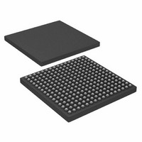
AD6636CBCZ Analog Devices Inc, AD6636CBCZ Datasheet - Page 12

AD6636CBCZ
Manufacturer Part Number
AD6636CBCZ
Description
IC DIGITAL DWNCONV 4CH 256CSPBGA
Manufacturer
Analog Devices Inc
Series
AD6636r
Datasheet
1.AD6636BCPCB.pdf
(80 pages)
Specifications of AD6636CBCZ
Rf Type
Cellular, CDMA2000, EDGE, GPRS, GSM
Number Of Mixers
1
Secondary Attributes
Down Converter
Current - Supply
450mA
Voltage - Supply
3 V ~ 3.6 V
Package / Case
256-CSPBGA
Brief Features
4/6 Independent Wideband Processing Channel, Quadrature Correction & DC Correction For Complex Input
Supply Voltage Range
1.7V To 1.9V
Operating Temperature Range
-40°C To +85°C
Ic Function
Digital Down Converter (DDC)
Rohs Compliant
Yes
Pin Count
256
Screening Level
Industrial
Package Type
CSPBGA
Lead Free Status / RoHS Status
Lead free / RoHS Compliant
Frequency
-
Gain
-
Noise Figure
-
Lead Free Status / Rohs Status
Compliant
Available stocks
Company
Part Number
Manufacturer
Quantity
Price
Company:
Part Number:
AD6636CBCZ
Manufacturer:
ADI
Quantity:
240
AD6636
Mnemonic
EXPB[0:2]
EXPC[0:2]
EXPD[0:2]
CLKA, CLKB
CLKC, CLKD
INA[0:15],
INB[0:15]
INC[0:15],
IND[0:15]
OUTPUT PORTS
PCLK
PA[0:15]
PACH[0:2]
PAIQ
PAGAIN
PAACK
PAREQ
PB[0:15]
PBCH[0:2]
PBIQ
PBGAIN
PBACK
PBREQ
PC[0:15]
PCCH[0:2]
PCIQ
PCGAIN
PCACK
PCREQ
MISC PINS
RESET
IRP
SYNC[0:3]
LVDS_RSET
EXT_FILTER
MICROPORT CONTROL
D[0:15]
A[0:7]
DS (RD)
DTACK (RDY)
R/W (WR)
MODE
CS
CPUCLK
CHIPID[0:3]
1
1
Type
Bidirectional
Bidirectional
Bidirectional
Input
Input
LVDS Input
LVDS Input
Bidirectional
Output
Output
Output
Output
Input
Output
Output
Output
Output
Output
Input
Output
Output
Output
Output
Output
Input
Output
Input
Output
Input
Input
Input
Bidirectional
Input
Input
Output
Input
Input
Input
Input
Input
Pin No.
D1, F3, G4
F4, D3, D2
D4, C2, F5
K1, L1
A6, A5
See Table 9
See Table 9
E16
See Table 9
G15, D16,
H12
H13
G13
H14
F15
See Table 9
C13, D11,
B14
D12
A14
E12
E11
See Table 9
M15, L14,
N15
P15
P16
L13
R16
P3
T2
B12, A12,
C10, B11
E4
R4
See Table 9
See Table 9
P4
M6
N4
T3
N5
R1
T4, R5, N6,
P6
Function
Exponent Bus Input Port B. Gain control output.
Exponent Bus Input Port C. Gain control output.
Exponent Bus Input Port D. Gain control output.
LVDS Differential Clock for LVDS_A Input Port (LVDS_CLKA+, LVDS_CLKA−).
LVDS Differential Clock for LVDS_C Input Port (LVDS_CLKC+, LVDS_CLKC−).
In LVDS input mode, INA[0:15] and INB[0:15] form a differential pair LVDS_A+[0:15]
(positive node) and LVDS_A–[0:15] (negative node), respectively.
In LVDS input mode, INC[0:15] and IND[0:15] form a differential pair LVDS_C+[0:15]
(positive node) and LVDS_C–[0:15] (negative node), respectively.
Parallel Output Port Clock. Master mode output, and slave mode input.
Parallel Output Port A Data Bus.
Channel Indicator Output Port A.
Parallel Port A I/Q Data Indicator. Logic 1 indicates I data on data bus.
Parallel Port A Gain Word Output Indicator. Logic 1 indicates gain word on data bus.
Parallel Port A Acknowledge (Active High).
Parallel Port A Request (Active High).
Parallel Output Port B Data Bus.
Channel Indicator Output Port B.
Parallel Port B I/Q Data Indicator. Logic 1 indicates I data on data bus.
Parallel Port B Gain Word Output Indicator. Logic 1 indicates gain word on data bus.
Parallel Port B Acknowledge (Active High).
Parallel Port B Request (Active High).
Parallel Output Port C Data Bus.
Channel Indicator Output Port C.
Parallel Port C I/Q Data Indicator. Logic 1 indicates I data on data bus.
Parallel Port C Gain Word Output Indicator. Logic 1 indicates gain word on data bus.
Parallel Port C Acknowledge (Active High).
Parallel Port C Request (Active High).
Master Reset (Active Low).
Interrupt Pin (Open Drain Output, Needs External Pull-Up Resistor 1 kΩ).
Synchronization Inputs. SYNC pins are independent of channels or input ports and
independent of each other.
LVDS Resistor Set Pin (Analog Pin). See Design Notes.
PLL Loop Filter (Analog Pin). See Design Notes.
Bidirectional Microport Data. This bus is three-stated when CS is high.
Microport Address Bus.
Active Low Data Strobe when MODE = 1. Active low read strobe when MODE = 0.
Active Low Data Acknowledge when MODE = 1. Microport status pin when MODE = 0.
Open drain output, needs external pull-up resistor 1 kΩ.
Read/Write Strobe when MODE = 1. Active low write strobe when MODE = 0.
Mode Select Pin. When SMODE = 0: Logic 0 = Intel mode; Logic 1 = Motorola mode.
When SMODE = 1: Logic 0 = SPI mode; Logic 1 = SPORT mode.
Active Low Chip Select. Logic 1 three-states the microport data bus.
Microport CLK Input (Input Only).
Chip ID Input Pins.
Rev. A | Page 12 of 80


