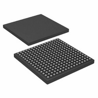
AD6636CBCZ Analog Devices Inc, AD6636CBCZ Datasheet - Page 49

AD6636CBCZ
Manufacturer Part Number
AD6636CBCZ
Description
IC DIGITAL DWNCONV 4CH 256CSPBGA
Manufacturer
Analog Devices Inc
Series
AD6636r
Datasheet
1.AD6636BCPCB.pdf
(80 pages)
Specifications of AD6636CBCZ
Rf Type
Cellular, CDMA2000, EDGE, GPRS, GSM
Number Of Mixers
1
Secondary Attributes
Down Converter
Current - Supply
450mA
Voltage - Supply
3 V ~ 3.6 V
Package / Case
256-CSPBGA
Brief Features
4/6 Independent Wideband Processing Channel, Quadrature Correction & DC Correction For Complex Input
Supply Voltage Range
1.7V To 1.9V
Operating Temperature Range
-40°C To +85°C
Ic Function
Digital Down Converter (DDC)
Rohs Compliant
Yes
Pin Count
256
Screening Level
Industrial
Package Type
CSPBGA
Lead Free Status / RoHS Status
Lead free / RoHS Compliant
Frequency
-
Gain
-
Noise Figure
-
Lead Free Status / Rohs Status
Compliant
Available stocks
Company
Part Number
Manufacturer
Quantity
Price
Company:
Part Number:
AD6636CBCZ
Manufacturer:
ADI
Quantity:
240
Hop with Soft Sync
The AD6636 can synchronize a change in NCO frequency
and/or phase offset of multiple channels or chips under
microprocessor control. The NCO hop hold-off counter, in
conjunction with the soft hop enable bit and the channel enable
bits, enables this synchronization.
To synchronize the hop of multiple channels via microprocessor
control:
1.
2.
3.
4.
Note that when using SPI or SPORT for programming these
registers, the last step in the above procedure needs to be
repeated. Therefore, the soft synchronization configuration
register is written twice.
Hop with Pin Sync
Four sync pins (0, 1, 2 and 3) provide very accurate synchro-
nization among channels. Each channel can be programmed to
look at any of the four sync pins.
To control the hop of channel NCO frequencies:
1.
2.
3.
4.
Write the NCO frequency register(s) or phase offset
register(s) to the new value.
Write the NCO frequency hold-off counter register(s) with
the appropriate value (greater than 0 and less than 2
Write 0x00 to the soft synchronization configuration
register.
Write the soft hop synchronization enable bit and the
corresponding soft sync channel enable bits high in the soft
synchronization configuration register. This starts the
countdown by the frequency hold-off counter. When the
count reaches 1, the new frequency and/or phase offset is
loaded into the NCO.
Write the NCO frequency register(s) or phase offset
register(s) to the new value.
Write the NCO frequency hold-off counter(s) to the
appropriate value (greater than 0 and less than 2
Program the channel NCO control registers to monitor the
appropriate SYNC pins.
Write the hop synchronization enable bit and SYNC pin
enable bits high in the pin synchronization configuration
register. This enables the countdown of the frequency
hold-off counter. When the reaches 1, the new frequency
and/or phase offset is loaded into the NCO.
16
).
16
).
Rev. A | Page 49 of 80
SERIAL PORT CONTROL
The AD6636 serial port allows all memory to be accessed
(programmed or readback) serially in one-byte words. Either
serial port or microport can be used (but not both) at any given
time. Serial port control is selected using the SMODE pin (0 =
microport, 1 = serial port). Two serial port modes are available.
An SPI-compatible port is provided as well as a SPORT. The
choice of SPI or SPORT mode is selected using the MODE pin
(0 = SPI, 1 = SPORT).
Each individual byte of serial data (address, instruction, and
data) may be shifted in either MSB first or LSB first using the
MSB_FIRST pin (1 = MSB first, 0 = LSB first). The serial chip
select ( SCS ) pin is brought low to access the device for serial
control. When the SCS pin is held high, serial programming is
inhibited.
Hardware Interface
The pins described in Table 26 comprise the physical interface
between the user’s programming device and the serial port of
the AD6636. All serial pins are inputs except for SDO, which is
an open-drain output and should be pulled high by an external
pull-up resistor (suggested value 1 kΩ).
A complete read or write cycle requires a minimum of three
bytes to transfer, consisting of address word, instruction word,
and data-word(s). As many as 127 data-words can be
transferred during a block transfer cycle. All address,
instruction, and data-word(s) must be formatted LSB first or
MSB first to match the state of the MSB_FIRST pin.
The first word for serial transfer is the internal register address.
In LSB first mode, the address is the lower-most address for the
block transfer (subsequent addresses are generated by internal
increment). In MSB first, the address is highest address for the
block transfer (subsequent addresses are generated by internal
decrement).
The second word of serial transfer contains a one-bit read/write
indicator (1 = read, 0 = write), and seven bits to define the
number of data bytes to be transferred (N). For a single data
byte transfer (N = 1); one byte is shifted into SDI for a write
transfer, or shifted out of SDO for a read transfer, and the cycle
is complete. For a block transfer, N write/read operations are
performed, and the internal register address increments
(MSB_FIRST = 0) or decrements (MSB_FIRST = 1) after each
data byte is clocked into SDI for a write operation, or after each
data byte is clocked out of SDO for a read operation.
AD6636


