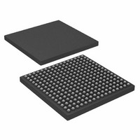
AD6636CBCZ Analog Devices Inc, AD6636CBCZ Datasheet - Page 29

AD6636CBCZ
Manufacturer Part Number
AD6636CBCZ
Description
IC DIGITAL DWNCONV 4CH 256CSPBGA
Manufacturer
Analog Devices Inc
Series
AD6636r
Datasheet
1.AD6636BCPCB.pdf
(80 pages)
Specifications of AD6636CBCZ
Rf Type
Cellular, CDMA2000, EDGE, GPRS, GSM
Number Of Mixers
1
Secondary Attributes
Down Converter
Current - Supply
450mA
Voltage - Supply
3 V ~ 3.6 V
Package / Case
256-CSPBGA
Brief Features
4/6 Independent Wideband Processing Channel, Quadrature Correction & DC Correction For Complex Input
Supply Voltage Range
1.7V To 1.9V
Operating Temperature Range
-40°C To +85°C
Ic Function
Digital Down Converter (DDC)
Rohs Compliant
Yes
Pin Count
256
Screening Level
Industrial
Package Type
CSPBGA
Lead Free Status / RoHS Status
Lead free / RoHS Compliant
Frequency
-
Gain
-
Noise Figure
-
Lead Free Status / Rohs Status
Compliant
Available stocks
Company
Part Number
Manufacturer
Quantity
Price
Company:
Part Number:
AD6636CBCZ
Manufacturer:
ADI
Quantity:
240
raised noise floor, phase dither should be employed. If a low
noise floor is desired and the higher spurs can be tolerated or
filtered by subsequent stages, then phase dither is not needed.
Amplitude Dither
This can be used to improve spurious performance of the NCO.
Amplitude dither is enabled by writing Logic 1 in the amplitude
dither enable bit of the NCO control register of the channel
under consideration. When this feature is enabled, random
amplitude is added to the LSBs of the sine and cosine
amplitudes. Amplitude dither improves performance by
randomizing the amplitude quantization errors within the
angular-to-Cartesian conversion of the NCO. This option can
reduce spurs at the expense of a slightly raised noise floor.
Amplitude and phase dither can be used together, separately, or
not at all.
NCO Frequency Hold-Off Register
When the NCO frequency registers are written by the
microport or serial port, data is passed to a shadow register.
Data can be moved to the main registers when the channel
comes out of sleep mode, or when a sync hop occurs. In either
event, a counter can be loaded with the NCO frequency hold-
off register value. The 16-bit unsigned integer counter starts
counting down, clocked by the input port clock selected at the
crossbar mux. When the counter reaches 0, the new frequency
value in the shadow register is written to the NCO frequency
register. Writing 1 in this hold-off register updates the NCO
frequency register as soon as the start sync or hop sync occurs.
See the Chip Synchronization section for details.
Phase Offset
The phase offset register can be written with a value that is
added as an offset to the phase accumulator of the NCO. This
16-bit register is interpreted as a 16-bit unsigned integer. A
0x0000 in this register corresponds to a 0 radian offset and a
0xFFFF corresponds to an offset of 2π × (1 − 1/2
This register allows multiple NCOs (multiple channels) to be
synchronized to produce complex sinusoids with a known and
steady phase difference.
Hop Sync
When the channel’s NCO frequency needs to be changed from
one frequency to a different frequency, a hop sync should be
issued to the channel. This feature is discussed in detail in the
Chip Synchronization section.
16
) radians.
Rev. A | Page 29 of 80
FIFTH-ORDER CIC FILTER
The signal processing stage immediately after the NCO is a CIC
filter stage. This stage implements a fixed-coefficient,
decimating, cascade integrated comb filter. The input rate to
this filter is the same as the data rate at the input port; the
output rate from this stage is dependent on the decimation factor.
The decimation ratio, M
(only integer values). The 5-bit word in the CIC decimation
register is used to set the CIC decimation factor. A binary value
of one less than the decimation factor is written into this
register. The decimation ratio of 1 can be achieved by bypassing
the CIC filter stage. The frequency response of the filter is given
by the following equations. The gain and pass-band droop of
the CIC should be calculated by these equations. Both parame-
ters can be offset in the RCF stage.
where:
f
S
between 0 and 20.
The attenuation of the data into the CIC stage should be
controlled in 6 dB increments. For the best dynamic range, S
should be set to the smallest value possible (lowest attenuation
possible) without creating an overflow condition. This can be
accomplished safely using the following equation, where
input_level is the largest possible fraction of the full-scale value
at the input port. This value is output from the NCO stage and
pipelined into the CIC filter.
Bypass
The fifth-order CIC filter can be bypassed when no decimation
is required of it. When it is bypassed, the scaling operation is
not performed. In bypass mode, the output of the CIC filter is
the same as the input of the CIC filter.
in
CIC
is the data input rate to the channel under consideration.
, the scale factor, is a programmable unsigned integer
OL
H
H
S
f
CIC
CIC
( )
( )
z
CIC
f
=
=
=
=
ceil
=
M
2
2
f
(
(
(
2
CIC
in
S
M
S
(
CIC
CIC
S
log
1
1
CIC
CIC
+
+
5
5
2
+5
)
5
)
(
×
M
×
)
×
⎛
⎜
⎜
⎝
⎛
⎜
⎜
⎜
⎜
⎜
⎝
CIC
input_leve
1
SIN
CIC
−
1 Z
5
SIN
Z
−
×
, can be programmed from 2 to 32
⎛
⎜
⎜
⎝
−
input_leve
M
M
⎛
⎜
⎜
⎝
−
CIC
1
π
CIC
f
in
f
l
f
⎞
⎟
⎟
⎠
in
×
5
⎞
⎟
⎟
⎠
f
⎞
⎟
⎟
⎠
l
)
⎞
⎟
⎟
⎟
⎟
⎟
⎠
)
5
−
5
AD6636
CIC


