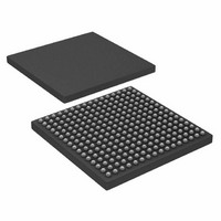
AD6636CBCZ Analog Devices Inc, AD6636CBCZ Datasheet - Page 62

AD6636CBCZ
Manufacturer Part Number
AD6636CBCZ
Description
IC DIGITAL DWNCONV 4CH 256CSPBGA
Manufacturer
Analog Devices Inc
Series
AD6636r
Datasheet
1.AD6636BCPCB.pdf
(80 pages)
Specifications of AD6636CBCZ
Rf Type
Cellular, CDMA2000, EDGE, GPRS, GSM
Number Of Mixers
1
Secondary Attributes
Down Converter
Current - Supply
450mA
Voltage - Supply
3 V ~ 3.6 V
Package / Case
256-CSPBGA
Brief Features
4/6 Independent Wideband Processing Channel, Quadrature Correction & DC Correction For Complex Input
Supply Voltage Range
1.7V To 1.9V
Operating Temperature Range
-40°C To +85°C
Ic Function
Digital Down Converter (DDC)
Rohs Compliant
Yes
Pin Count
256
Screening Level
Industrial
Package Type
CSPBGA
Lead Free Status / RoHS Status
Lead free / RoHS Compliant
Frequency
-
Gain
-
Noise Figure
-
Lead Free Status / Rohs Status
Compliant
Available stocks
Company
Part Number
Manufacturer
Quantity
Price
Company:
Part Number:
AD6636CBCZ
Manufacturer:
ADI
Quantity:
240
AD6636
8-Bit Hex
Address
0x97
0x9B
0x9F
0xA3
0xA7
0xAB
0xAF
0xB3
0xB7
0xBB
Output Port Register Map—Addresses 0xBC to 0xE7
0xBF
0xC3
0xC7
0xCB
0xCF
0xD3
0xD7
0xDB
0xDF
0xE3
0xE7
GLOBAL REGISTER MAP
Chip I/O Access Control Register <7:0>
<7>: Synchronous Microport Bit. When this bit is set, the
microport assumes that its controls signals (such as R/ W , DS ,
and CS ) are synchronous to the CPUCLK. When cleared,
asynchronous control signals are assumed and the microport
control signals are resynchronized with CPUCLK inside the
AD6636 part. Synchronous microport (when bit is set) has the
advantage of requiring a fewer number of clock cycles for
read/write access.
<6>: This bit is open.
<5:2>: Chip ID Bits. The chip ID bits are used to compare
against the chip ID input pins, enabling or disabling I/O access
for this specific chip. When more than one AD6636 part is
sharing the microport, different CHIPID pins can be used to
differentiate among the parts. A particular part gives I/O access
only when the CHIPID pins have the same value as these chip
ID bits.
<1>: This bit is open.
<0>: Byte Mode Bit. The byte mode bit selects the bit width for
the microport operation. Table 31 shows details.
Byte 3
Open<15:12>, CRCF Control Register<11:0>
Open<15:0>
Open<7:0>
Open<15:11>, AGC Control Register<10:0>
Open<15:12>, AGC Update Decimation<11:0>
Open<15:12>, AGC Error Threshold <11:0>
Open<7:0>
Open<7:0>
Open<7:0>
Open <15:0>
Open<7:0>
Open<15:0>
AGC0, I Output<15:0> (Read-Only)
AGC1, I Output <15:0> (Read-Only)
AGC2, I Output <15:0> (Read-Only)
AGC3, I Output <15:0> (Read-Only)
AGC4, I Output <15:0> (Read-Only)
AGC5, I Output <15:0> (Read-Only)
Open<15:12>, AGC0 RSSI Output<11:0> (Read-Only)
Open<15:12>, AGC2 RSSI Output<11:0> (Read-Only)
Open<15:12>, AGC4 RSSI Output<11:0> (Read-Only)
Byte 2
Open<23:20>, CRCF Coefficient Memory <19:0>
AGC Desired Level<7:0>
BIST I Path Signature Register<23:0> (Read-Only, Default 0xAD6636)
BIST Q Path Signature Register<23:0> (Read-Only, Default 0xAD6636)
Parallel Port Output Control <23:0>
Rev. A | Page 62 of 80
Byte 1
Open <7:6>, CRCF
Coefficient Offset<5:0>
Open <7:6>, CRCF
Final Address<5:0>
AGC Hold-Off Register<15:0>
Open<15:12>, AGC Signal Gain <11:0>
Open<7:6>, AGC Average
Samples<5:0>
AGC Loop Gain2 <7:0>
BIST Control <15:0>
Open<15:10>, Output Port Control <9:0>
AGC0, Q Output <15:0> (Read-Only)
AGC1, Q Output <15:0> (Read-Only)
AGC2, Q Output <15:0> (Read-Only)
AGC3, Q Output <15:0> (Read-Only)
AGC4, Q Output <15:0> (Read-Only)
AGC5, Q Output <15:0> (Read-Only)
Open<15:12>, AGC1 RSSI Output<11:0> (Read-Only)
Open<15:12>, AGC3 RSSI Output<11:0> (Read-Only)
Open<15:12>, AGC5 RSSI Output<11:0> (Read-Only)
Table 31. Microport Data Bus Width Selection
Chip Access
Control Register <0>
0 (default)
1
Channel I/O Access Control Register <5:0>
These bits enable/disable the channel I/O access capability.
<5>: Channel 5 Access Bit. When the Channel 5 access bit is set
to Logic 1, any I/O write operation (from either the microport
or the serial port) that addresses a register located within the
channel register map updates the Channel 5 registers. Similarly,
for a read operation, the contents of the desired address in the
channel register map are output when this bit is set to Logic 1.
<4>: Channel 4 Access Bit. Similar to Bit <5> for Channel 4.
<3>: Channel 3 Access Bit. Similar to Bit <5> for Channel 3.
<2>: Channel 2 Access Bit. Similar to Bit <5> for Channel 2.
<1>: Channel 1 Access Bit. Similar to Bit <5> for Channel 1.
<0>: Channel 0 Access Bit. Similar to Bit <5> for Channel 0.
Byte 0
Open<7>, CRCF Taps
<6:0>
Open <7:6>, CRCF Start
Address<5:0>
AGC Pole Location
<7:0>
AGC Loop Gain1 <7:0>
Microport Data Bus Bit Width
8-bit mode, using D<7:0>
16-bit mode, using D<15:0>
8-Bit Hex
Address
0x94
0x98
0xA8
0xB0
0xB4
0xBC
0xC0
0xC4
0xDC
0xE0
0xE4
0x9C
0xA0
0xA4
0xAC
0xB8
0xC8
0xCC
0xD0
0xD4
0xD8


