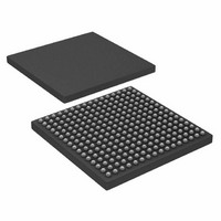
AD6636CBCZ Analog Devices Inc, AD6636CBCZ Datasheet - Page 77

AD6636CBCZ
Manufacturer Part Number
AD6636CBCZ
Description
IC DIGITAL DWNCONV 4CH 256CSPBGA
Manufacturer
Analog Devices Inc
Series
AD6636r
Datasheet
1.AD6636BCPCB.pdf
(80 pages)
Specifications of AD6636CBCZ
Rf Type
Cellular, CDMA2000, EDGE, GPRS, GSM
Number Of Mixers
1
Secondary Attributes
Down Converter
Current - Supply
450mA
Voltage - Supply
3 V ~ 3.6 V
Package / Case
256-CSPBGA
Brief Features
4/6 Independent Wideband Processing Channel, Quadrature Correction & DC Correction For Complex Input
Supply Voltage Range
1.7V To 1.9V
Operating Temperature Range
-40°C To +85°C
Ic Function
Digital Down Converter (DDC)
Rohs Compliant
Yes
Pin Count
256
Screening Level
Industrial
Package Type
CSPBGA
Lead Free Status / RoHS Status
Lead free / RoHS Compliant
Frequency
-
Gain
-
Noise Figure
-
Lead Free Status / Rohs Status
Compliant
Available stocks
Company
Part Number
Manufacturer
Quantity
Price
Company:
Part Number:
AD6636CBCZ
Manufacturer:
ADI
Quantity:
240
DESIGN NOTES
The following guidelines describe circuit connections, layout
requirements, and programming procedures for the AD6636.
The designer should review these guidelines before starting the
system design and layout.
• The AD6636 requires the following power-up sequence. The
• Input clocks (CLKA, CLKB, CLKC, CLKD) and input port
• When the ADC output has less than 16 bits of resolution,
• The number format used in this part is twos complement. All
• In both microport and serial port operation, the DTACK
• A simple RC circuit is used on the EXT_FILTER pin to
VDDCORE (1.8 V) must settle into nominal voltage levels
before the VDDIO attains the minimum. This ensures that,
on power-up, the JTAG does not take control of the I/O pins.
pins (INA[15:0] to IND[15:0], EXPA[2:0] to EXPD[2:0]) are
not 5 V tolerant. Care should be taken to drive these pins
within the limits of VDDIO (3.0 V to 3.6 V).
it should be connected to the MSBs of the input port (MSB-
justified). The remaining LSBs should be connected to
ground.
input ports and output ports use twos complement data
format. The formats for individual internal registers are given
in the memory map description of these registers.
(RDY, SDO) pin is an open-drain output and therefore
should be pulled high externally using a pull-up resister.
The recommended value for the pull-up resistor is from
1 kΩ to 5 kΩ.
balance the internal RC circuit on this pin and maintain a
good PLL clock lock. The recommended circuit is shown in
Figure 59, with the RC circuit connected to VDDCORE. This
RC circuit should be placed as close as possible to the
AD6636 part. This layout ensures that the PLL clock is void
of noise and spurs and the PLL lock is maintained closely.
Figure 58. DTACK , SDO Pull-Up Resistor Circuit
3.3V
1kΩ
DTACK (RDY, SDO)
AD6636
Rev. A | Page 77 of 80
• By default, the PLL CLK is disabled. It can be enabled by
• The LVDS_RSET pin is used to calibrate the current in the
• To reset the AD6636 part, the user needs to provide a
• Most AD6636 pins are driven by both JTAG circuitry and
programming the PLL multiplier and divider bits in the ADC
CLK control register. When the PLL CLK is enabled by
programming this register, it takes between 50 μs and 200 μs
to settle. While the PLL loop settles, the voltage at the
EXT_FILTER pin increases from 0 V to VDDCORE (1.8 V)
and settles there. Channel registers and output port registers
(Address 0x68 to Address 0xE7) should not be programmed
before the PLL loop settles.
LVDS pads. The recommended circuit for this pin is shown
in Figure 60. This resistor should be placed as close as
possible to the AD6636 part. If CMOS mode input is used,
this resistor is not required.
minimum pulse of 30 ns to the RESET pin. The RESET pin
should be connected to GND (or pulled low) during power-
up of the part. The RESET pin can be pulled high after the
power supplies have settled to nominal values (1.8 V and
3.3 V). At this point, a pulse (pull low and high again) should
be provided to give a RESET to the part.
normal function circuitry specific to each pin. TRST is the
reset pin for JTAG. When TRST is pulled low, JTAG is in
reset and all pins function in normal mode (driven by the
functional circuit). If JTAG is not used in the design, the
TRST pin should be pulled low at all times.
Figure 60. LVDS_RSET Circuit for LVDS Calibration
VDDCORE (1.8V)
Figure 59. EXT_FILTER Circuit for PLL Clock
10kΩ
0.01μF
250Ω
LVDS_RSET
EXT_FILTER
AD6636
AD6636
AD6636


