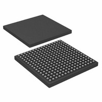
AD6636CBCZ Analog Devices Inc, AD6636CBCZ Datasheet - Page 74

AD6636CBCZ
Manufacturer Part Number
AD6636CBCZ
Description
IC DIGITAL DWNCONV 4CH 256CSPBGA
Manufacturer
Analog Devices Inc
Series
AD6636r
Datasheet
1.AD6636BCPCB.pdf
(80 pages)
Specifications of AD6636CBCZ
Rf Type
Cellular, CDMA2000, EDGE, GPRS, GSM
Number Of Mixers
1
Secondary Attributes
Down Converter
Current - Supply
450mA
Voltage - Supply
3 V ~ 3.6 V
Package / Case
256-CSPBGA
Brief Features
4/6 Independent Wideband Processing Channel, Quadrature Correction & DC Correction For Complex Input
Supply Voltage Range
1.7V To 1.9V
Operating Temperature Range
-40°C To +85°C
Ic Function
Digital Down Converter (DDC)
Rohs Compliant
Yes
Pin Count
256
Screening Level
Industrial
Package Type
CSPBGA
Lead Free Status / RoHS Status
Lead free / RoHS Compliant
Frequency
-
Gain
-
Noise Figure
-
Lead Free Status / Rohs Status
Compliant
Available stocks
Company
Part Number
Manufacturer
Quantity
Price
Company:
Part Number:
AD6636CBCZ
Manufacturer:
ADI
Quantity:
240
AD6636
<15>: Port B Append RSSI Bit. When this bit is set, an RSSI
word is appended to every I/Q output sample, irrespective of
whether or not the RSSI word is updated in the AGC. When
this bit is cleared, an RSSI word is appended to an I/Q output
sample when the RSSI word is updated only. The RSSI word is
not output for subsequent I/Q samples until the next time the
RSSI is updated in the AGC.
<14>: Port B, Data Format Bit. When this bit is set, the port is
configured for 8-bit parallel I/Q mode. When this bit is cleared,
the port is configured for 16-bit interleaved I/Q mode. See the
Parallel Port Output section.
<13>: Port B, AGC5 Enable Bit. When this bit is set, AGC5 data
(I/Q data) is output on parallel output Port A (data bus). When
this bit is cleared, AGC5 data does not appear on output Port C.
<12>: Port B, AGC4 Enable Bit. Similar to Bit <13> for AGC4.
<11>: Port B, AGC3 Enable Bit. Similar to Bit <13> for AGC3.
<10>: Port B, AGC2 Enable Bit. Similar to Bit <13> for AGC2.
<9>: Port B, AGC1 Enable Bit. Similar to Bit <13> for AGC1.
<8>: Port B, AGC0 Enable Bit. Similar to Bit <13> for AGC0.
<7>: Port A Append RSSI Bit. When this bit is set, an RSSI word
is appended to every I/Q output sample, irrespective of whether
or not the RSSI word is updated in the AGC. When this bit is
cleared, an RSSI word is appended to an I/Q output sample only
when the RSSI word is updated. The RSSI word is not output for
subsequent I/Q samples until the next time RSSI is updated
again in the AGC.
<6>: Port A, Data Format Bit. When this bit is set, the port is
configured for 8-bit parallel I/Q mode. When this bit is cleared,
the port is configured for 16-bit interleaved I/Q mode. See the
Parallel Port Output section.
<5>: Port A, AGC5 Enable Bit. When this bit is set, AGC5 data
(I/Q data) is output on parallel output Port A (data bus). When
this bit is cleared, AGC5 data does not appear on output Port C.
<4>: Port A, AGC4 Enable Bit. Similar to Bit <5> for AGC4.
<3>: Port A, AGC3 Enable Bit. Similar to Bit <5> for AGC3.
<2>: Port A, AGC2 Enable Bit. Similar to Bit <5> for AGC2.
<1>: Port A, AGC1 Enable Bit. Similar to Bit <5> for AGC1.
<0>: Port A, AGC0 Enable Bit. Similar to Bit <5> for AGC0.
Rev. A | Page 74 of 80
Output Port Control <9:0>
<9:8>: PCLK Divisor Bits. When a parallel port is in master
mode, the PCLK is derived from the PLL_CLK. These bits
define the value of the divisor used to divide the PLL_CLK to
obtain the PCLK. These bits are don’t care in slave mode.
Table 44. PCLK Divisor Bits
PCLK Divisor <9:8>
00
01
10
11
<7>: PCLK Master Mode Bit. When the PCLK master mode bit
is set, the PCLK pin is configured as an output and the PCLK is
driven by the PLL_CLK. Data is transferred out of the AD6636
synchronous to this output clock. When this bit is cleared, the
PCLK pin is configured as an input. The user is required to
provide a PCLK, and data is transferred out of the AD6636
synchronous to this input clock. On power-up, this bit is cleared
to avoid contention on the PCLK pin.
<6:4>: Complex Control Bits. These bits are described in
Table 45.
Table 45. Complex Control Bits
Complex Control <6:4>
000
001
010
011
101
110
111
No complex filters
Str0/Str1 combined
Str0/Str1 combined,
Str2/Str3 combined
Str0/Str1 combined,
Str2/Str3 combined,
Str4/Str5 combined
Str0/Str1 combined
Str0/Str1 combined,
Str2/Str3 combined
Str0/Str1 combined,
Str2/Str3 combined,
Str4/Str5 combined
Comment
Stream control register controls
AGC usage.
Ch 0 and Ch 1 form a complex
filter.
Ch 0 and Ch 1 form a complex
filter; Ch 2 and Ch 3 form a
complex filter.
Ch 0 and Ch 1 form a complex
filter; Ch 2 and Ch 3 form a
complex filter; Ch 4 and Ch 5
form a complex filter.
Ch 0 and Ch 1 form a biphase
filter.
Ch 0 and Ch 1 form a biphase
filter; Ch 2 and Ch 3 to form a
biphase filter.
Ch 0 and Ch 1 to form a biphase
filter; Ch 2 and Ch 3 to form a
biphase filter; Ch 4 and Ch 5 to
form a biphase filter.
Divisor Value
1
2
4
8


