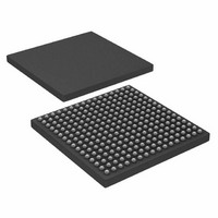
AD6636CBCZ Analog Devices Inc, AD6636CBCZ Datasheet - Page 59

AD6636CBCZ
Manufacturer Part Number
AD6636CBCZ
Description
IC DIGITAL DWNCONV 4CH 256CSPBGA
Manufacturer
Analog Devices Inc
Series
AD6636r
Datasheet
1.AD6636BCPCB.pdf
(80 pages)
Specifications of AD6636CBCZ
Rf Type
Cellular, CDMA2000, EDGE, GPRS, GSM
Number Of Mixers
1
Secondary Attributes
Down Converter
Current - Supply
450mA
Voltage - Supply
3 V ~ 3.6 V
Package / Case
256-CSPBGA
Brief Features
4/6 Independent Wideband Processing Channel, Quadrature Correction & DC Correction For Complex Input
Supply Voltage Range
1.7V To 1.9V
Operating Temperature Range
-40°C To +85°C
Ic Function
Digital Down Converter (DDC)
Rohs Compliant
Yes
Pin Count
256
Screening Level
Industrial
Package Type
CSPBGA
Lead Free Status / RoHS Status
Lead free / RoHS Compliant
Frequency
-
Gain
-
Noise Figure
-
Lead Free Status / Rohs Status
Compliant
Available stocks
Company
Part Number
Manufacturer
Quantity
Price
Company:
Part Number:
AD6636CBCZ
Manufacturer:
ADI
Quantity:
240
Motorola (MNM) Mode
The programming port performs synchronous Motorola-style
reads and writes on the positive edge of CPUCLK when RESET
is inactive (active low signal). The A[7:0] bus provides the
address to access and the D[15:0] bus (D[7:0], if the 8-bit data
bus is used) is externally driven with data during a write (driven
by the AD6636 during a read). Motorola mode uses the R/ W
line to indicate the type of access (Logic 1 = read, Logic 0 =
write), and the active-low data strobe ( DS ) signal is used to
indicate valid data.
The chip select ( CS ) is an active-low input that signals when an
access is active on its programming port pins. When the
read/write cycle is complete, the AD6636 drives DTACK low.
The DTACK signal goes high again after either the CS or DS
signal is driven high. Because the DTACK pin is an open-drain
output with a weak internal pull-up resistor (70 kΩ), an
external pull-up resistor is recommended (see Figure 58).
Figure 15 and Figure 16 are the timing diagrams for read and
write cycles using the microport in MNM mode. Do not read or
write, to or from, addresses beyond those defined by the
memory map (Address 0xE8 to Address 0xFF). Attempting to
access these addresses causes the bus to hang because DTACK
does not go high to signal the end of the access.
For an asynchronous write operation on the Motorola mode
microport, the CPUCLK should be running. Set up the data and
address buses. Pull the R/ W and DS signals low and then pull
the CS signal low. The DTACK goes low after a few clock cycles
to indicate that the write access is complete and that CS can be
pulled high to disable the microport. For an asynchronous read
operation on the Motorola mode microport, set up the address
bus and three-state the data bus. Pull the RD signal low and
then pull the CS signal low. The DTACK goes low after a few
clock cycles to indicate that valid data is on the data bus.
Accessing Multiple AD6636 Devices
If multiple AD6636 devices are on a single board, the microport
pins for these devices can be shared. In this configuration, a
single programming device (DSP, FPGA, or microcontroller)
can program all AD6636 devices connected to it.
Each AD6636 has four CHIPID pins that can be connected in
16 different ways. During a write/read access, the internal
circuitry checks to see if the CHIPID bits in the chip I/O access
control register (Address 0x02) are the same as the logic levels
of the CHIPID pins (hardwired to the part). If the CHIPID bits
and the CHIPID pins have the same value, then a write/read
access is completed; otherwise, the access is ignored.
To program multiple devices using the same microport control
and data buses, the devices should have separate CHIPID pin
configurations. A write/read access can be made on the
intended chip only; all other chips would ignore the access.
Rev. A | Page 59 of 80
JTAG BOUNDARY SCAN
The AD6636 supports a subset of the IEEE Standard 1149.1
specification. For details of the standard, see the IEEE Standard
Test Access Port and Boundary-Scan Architecture, an IEEE-1149
publication.
The AD6636 has five pins associated with the JTAG interface.
These pins, listed in Table 28, are used to access the on-chip test
access port. All input JTAG pins are pull-up except for TCLK,
which is pull-down.
Table 28. Boundary Scan Test Pins
Mnemonic
TRST
TCLK
TMS
TDI
TDO
The AD6636 supports three op codes, listed in Table 29. These
instructions set the mode of the JTAG interface.
Table 29. Boundary Scan Op Codes
Instruction
BYPASS
SAMPLE/PRELOAD
EXTEST
A BSDL file for this device is available. Contact sales for more
information.
EXTEST (2'b00)
Places the IC into an external boundary-test mode and selects
the boundary-scan register to be connected between TDI and
TDO. During this operation, the boundary-scan register is
accessed to drive-test data off-chip via boundary outputs and
receive test data off-chip from boundary inputs.
SAMPLE/PRELOAD (2'b01)
Allows the IC to remain in normal functional mode and selects
the boundary-scan register to be connected between TDI and
TDO. The boundary-scan register can be accessed by a scan
operation to take a sample of the functional data entering and
leaving the IC. Also, test data can be preloaded into the
boundary scan register before an EXTEST instruction.
BYPASS (2'b11)
Allows the IC to remain in normal functional mode and selects
a 1-bit bypass register between TDI and TDO. During this
instruction, serial data is transferred from TDI to TDO without
affecting operation of the IC.
Description
Test Access Port Reset
Test Clock
Test Access Port Mode Select
Test Data Input
Test Data Output
Op Code
11
01
00
AD6636


