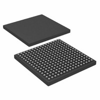
AD6636CBCZ Analog Devices Inc, AD6636CBCZ Datasheet - Page 35

AD6636CBCZ
Manufacturer Part Number
AD6636CBCZ
Description
IC DIGITAL DWNCONV 4CH 256CSPBGA
Manufacturer
Analog Devices Inc
Series
AD6636r
Datasheet
1.AD6636BCPCB.pdf
(80 pages)
Specifications of AD6636CBCZ
Rf Type
Cellular, CDMA2000, EDGE, GPRS, GSM
Number Of Mixers
1
Secondary Attributes
Down Converter
Current - Supply
450mA
Voltage - Supply
3 V ~ 3.6 V
Package / Case
256-CSPBGA
Brief Features
4/6 Independent Wideband Processing Channel, Quadrature Correction & DC Correction For Complex Input
Supply Voltage Range
1.7V To 1.9V
Operating Temperature Range
-40°C To +85°C
Ic Function
Digital Down Converter (DDC)
Rohs Compliant
Yes
Pin Count
256
Screening Level
Industrial
Package Type
CSPBGA
Lead Free Status / RoHS Status
Lead free / RoHS Compliant
Frequency
-
Gain
-
Noise Figure
-
Lead Free Status / Rohs Status
Compliant
Available stocks
Company
Part Number
Manufacturer
Quantity
Price
Company:
Part Number:
AD6636CBCZ
Manufacturer:
ADI
Quantity:
240
Coefficient Offset
More than one set of filter coefficients can be loaded into the
coefficient RAM at any given time (given sufficient RAM
space). The coefficient offset can be used in this case to access
the two or more different filters. By changing the coefficient
offset, the filter coefficients being accessed can be changed on
the fly. This decimal offset value is programmed in the DRCF
coefficient offset register. When this value is changed during the
calculation of a particular output data sample, the sample
calculation is completed using the old coefficients, and the new
coefficient offset from the next data sample calculation is used.
Decimation Phase
When more than one channel of AD6636 is used to process one
carrier, polyphase implementation of corresponding channels’
DRCF or CRCF is possible using the decimation phase feature.
This feature can only be used under certain conditions. The
decimation phase is programmed using the 4-bit DRCF
decimation phase word of the DRCF control register.
Maximum Number of Taps Calculated
The output rate of the DRCF filter is given by
where:
f
filter.
M
The DRCF filter consists of two multipliers (one each for the
I and Q paths). Each multiplier, working at the high speed clock
rate (PLL clock), can do one multiply (or one tap) per high
speed clock cycle. Therefore, the maximum number of filter
taps that can be calculated (symmetrical or asymmetrical filter)
is given by
where:
f
the PLL clock multiplier.
f
MRCF
PLLCLK
DRCF
DRCF
is the output rate of the DRCF filter calculated above.
is the data rate out of the MRCF filter and into the DRCF
Maximum
f
is the high speed internal processing clock generated by
DRCF
is the decimation rate in the DRCF filter.
=
M
f
MRCF
DRCF
Number
of
Taps
=
ceil
⎛
⎜
⎜
⎝
f
f
PLLCLK
DRCF
⎞
⎟
⎟
⎠
−
1
Rev. A | Page 35 of 80
Programming DRCF Registers for an Asymmetrical Filter
To program the DRCF registers for an asymmetrical filter:
1.
2.
3.
4.
5.
6.
7.
Note that each write or read access increments the internal
RAM address. Therefore, all coefficients should be read first
before reading them back. Also, for debugging purposes, each
RAM address can be written individually by making the start
address and stop address the same. Therefore, to program one
RAM location, the user writes the address of the RAM location
to both the start and stop address registers, and then writes the
coefficient memory register.
Programming DRCF Registers for a Symmetric Filter
To program the DRCF registers for a symmetrical filter:
1.
2.
3.
4.
Write NTAPS – 1 in the DRCF taps register, where NTAPS
is the number of filter taps. The absolute maximum value
for NTAPS is 64 in asymmetrical filter mode.
Write 0 to the DRCF coefficient offset register.
Write 0 to the symmetrical filter bit in the DRCF control
register.
Write the start address for the coefficient RAM, typically
equal to the coefficient offset register, in the DRCF start
address register.
In the DRCF stop address register, write the stop address
for the coefficient RAM, typically equal to
Write all coefficients in reverse order (start with last
coefficient) to the DRCF coefficient memory register. If in
8-bit microport mode or serial port mode, write the lower
byte of the memory register first and then the higher byte.
After each write access to the DRCF coefficient memory
register, the internal RAM address is incremented starting
with the start address and ending with the stop address.
Write NTAPS – 1 in the DRCF taps register, where NTAPS
is the number of filter taps. The absolute maximum value
for NTAPS is 128 in symmetric filter mode.
Write ceil(64 – NTAPS/2) to the DRCF coefficient offset
register, where the ceil function takes the closest integer
greater than or equal to the argument.
Write 1 to the symmetrical filter bit in the DRCF control
register.
Write the start address for the coefficient RAM, typically
equal to coefficient offset register, in the DRCF start
address register.
Coefficient Offset + NTAPS − 1
AD6636


