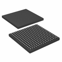
AD6636CBCZ Analog Devices Inc, AD6636CBCZ Datasheet - Page 60

AD6636CBCZ
Manufacturer Part Number
AD6636CBCZ
Description
IC DIGITAL DWNCONV 4CH 256CSPBGA
Manufacturer
Analog Devices Inc
Series
AD6636r
Datasheet
1.AD6636BCPCB.pdf
(80 pages)
Specifications of AD6636CBCZ
Rf Type
Cellular, CDMA2000, EDGE, GPRS, GSM
Number Of Mixers
1
Secondary Attributes
Down Converter
Current - Supply
450mA
Voltage - Supply
3 V ~ 3.6 V
Package / Case
256-CSPBGA
Brief Features
4/6 Independent Wideband Processing Channel, Quadrature Correction & DC Correction For Complex Input
Supply Voltage Range
1.7V To 1.9V
Operating Temperature Range
-40°C To +85°C
Ic Function
Digital Down Converter (DDC)
Rohs Compliant
Yes
Pin Count
256
Screening Level
Industrial
Package Type
CSPBGA
Lead Free Status / RoHS Status
Lead free / RoHS Compliant
Frequency
-
Gain
-
Noise Figure
-
Lead Free Status / Rohs Status
Compliant
Available stocks
Company
Part Number
Manufacturer
Quantity
Price
Company:
Part Number:
AD6636CBCZ
Manufacturer:
ADI
Quantity:
240
AD6636
MEMORY MAP
READING THE MEMORY MAP TABLE
Each row in the memory map table has four address locations.
The memory map is roughly divided into four regions: global
register map (Address 0x00 to Address 0x0B), input port
register map (Address 0x0C to Address 0x67), channel register
map (Address 0x68 to Address 0xBB), and output port register
map (Address 0xBC to Address 0xE7). The channel register
map is shared by all six channels and access to individual
channels is given by the channel I/O access control register
(Address 0x02).
In the memory map (see Table 30), the addresses are given in
the right column. The column with the heading Byte 0 has the
address given in the right column. The column Byte 1 has the
address given by 1 more than the address listed in the right
column (address offset of 1). Similarly, the address offset for the
Byte 2 column is 2, and for the Byte 3 column is 3. For example,
the second row lists 0x04 as the address in the right column.
The pin synchronization configuration register has
Address 0x04, the soft synchronization configuration register
has Address 0x05, and the LVDS control register lists
Address 0x07 and Address 0x06.
Bit Format
All registers are in little-endian format. For example, if a register
takes 24 bits or three address locations, then the most
significant byte is at the highest address location and the least
significant byte is at a lowest address location. In all registers,
the least significant bit is Bit 0 and the most significant bit is
Bit 7. For example, the NCO frequency <31:0> register is
32 bits wide. Bit 0 (LSB) of this register is written at Bit 0 of
Address 0x70 and Bit 32 (MSB) of this register is written at
Bit 7 of Address 0x73.
When referring to a register that takes up multiple address
locations, it is referred to by the address location of the most
significant byte of the register. For example, the text reads
“Port A dwell timer at Address 0x2A. ” Note that only the four
most significant bits of this register are at this location, and this
register also takes up Address 0x29 and Address 0x28.
Rev. A | Page 60 of 80
Open Locations
All locations marked as open are currently not used. When
required, these locations should be written with 0s. Writing to
these locations is required only when part of an address location
is open (for example, Address 0x78). If the whole address
location is open (for example, Address 0x00), then this address
location does not need to be written. If the open locations are
readback using the microport or the serial port, the readback
value is undefined (each bit can be independently 1 or 0), and
these bits have no significance.
If an address location has more than one register or has one
register with some open bits, then the order of these registers is
as given in the table.
For example, Address 0x33: Open <7:5>, Port A Signal Monitor
<4:0>. The open <7:5> is located at Bits <7:5>, and the Port A
signal monitor <4:0> is located at Bits <4:0>.
Another example is Address 0x35: Open <15:10>, Port A Upper
Threshold <9:0> Here, Bits <7:2> of Address 0x35 are open
<15:10>. Bits <1:0> of Address 0x35 and Bits <7:0> of
Address 0x34 make up the Port A upper threshold <9:0>
register (Bit 1 of Address 0x35 is the MSB of the Port A upper
threshold register).
Default Values
When coming out of reset, some of the address locations (but
not all) are loaded with default values. When available, the
default values for the registers are given in the table. If the
default value is not listed, then these address locations are in an
undefined state (Logic 0 or Logic 1) on RESET .
Logic Levels
In the explanation of various registers, bit is set is synonymous
with bit is set to Logic 1 or writing Logic 1 for the bit. Similarly
clear a bit is synonymous with bit is set to Logic 0 or writing
Logic 0 for the bit.


