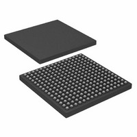
AD6636CBCZ Analog Devices Inc, AD6636CBCZ Datasheet - Page 50

AD6636CBCZ
Manufacturer Part Number
AD6636CBCZ
Description
IC DIGITAL DWNCONV 4CH 256CSPBGA
Manufacturer
Analog Devices Inc
Series
AD6636r
Datasheet
1.AD6636BCPCB.pdf
(80 pages)
Specifications of AD6636CBCZ
Rf Type
Cellular, CDMA2000, EDGE, GPRS, GSM
Number Of Mixers
1
Secondary Attributes
Down Converter
Current - Supply
450mA
Voltage - Supply
3 V ~ 3.6 V
Package / Case
256-CSPBGA
Brief Features
4/6 Independent Wideband Processing Channel, Quadrature Correction & DC Correction For Complex Input
Supply Voltage Range
1.7V To 1.9V
Operating Temperature Range
-40°C To +85°C
Ic Function
Digital Down Converter (DDC)
Rohs Compliant
Yes
Pin Count
256
Screening Level
Industrial
Package Type
CSPBGA
Lead Free Status / RoHS Status
Lead free / RoHS Compliant
Frequency
-
Gain
-
Noise Figure
-
Lead Free Status / Rohs Status
Compliant
Available stocks
Company
Part Number
Manufacturer
Quantity
Price
Company:
Part Number:
AD6636CBCZ
Manufacturer:
ADI
Quantity:
240
AD6636
Figure 44 to Figure 47 illustrate a three byte block transfer
through the serial port. Read and write operations with
MSB_FIRST high and low are shown. Note that the figures
show the sequence for write/read transfer, and actual data
should be shifted in or out based upon the status of the
Table 26. Serial Port Pins
Pin
SCLK
MSB_FIRST
STFS
SRFS
SDI
SDO
SCS
SMODE
MODE
MSBFIRST
MSBFIRST
MODE
MODE
SDO
SDO
SCS
SCS
SDI
SDI
Function
Serial Clock in Both SPI and SPORT Modes. Should have a rise/fall time of 3 ns maximum.
Indicates whether the first bit shifted in or out of the serial port is the MSB (1) or LSB (0) for both instruction and
data-words. Also indicates if the first instruction word (address) is a block start or a block end for multiple byte
transfers. This pin also controls the functionality when programming indirectly addressed registers.
Serial Transmit Frame Sync in SPORT Mode. STFS is not used in SPI mode.
Serial Receive Frame Sync in SPORT Mode. SRFS is not used in SPI mode.
Serial Data Input in Both Modes. Serial data is clocked in on the rising edge of SCLK.
Serial Data Output in Both Modes. Serial data is clocked out on the rising edge of SCLK.
Active-Low Serial Chip Select in Both Modes.
Serial Mode. Part is programmed through the serial port when this pin is high.
Mode Pin. Selects between SPI (0) and SPORT (1) modes.
Figure 44. Serial Write of Three Bytes with MSB_FIRST = 1 (All Words are Written MSB First)
BLOCK END ADDRESS WR + COUNT (3)
Figure 45. Serial Write of Three Bytes with MSB_FIRST = 0 (All Words are Written LSB First)
BLOCK START
ADDRESS
0xaa
0xaa
WR + COUNT (3)
0x03
0x03
Rev. A | Page 50 of 80
DATA TO BLOCK START
DATA TO BLOCK END
ADDRESS
ADDRESS
aa
aa
MSB_FIRST pin. The operation details are common to both SPI
and SPORT modes, except for the use of framing signals and
timing. Individual mode details follow. In single-byte transfer
mode, the count in the second byte is reduced to 1, and the
number of data bytes is reduced to 1.
DATA TO BLOCK START
DATA TO BLOCK END
ADDRESS – 1
ADDRESS + 1
aa – 1
aa + 1
DATA TO BLOCK START
DATA TO BLOCK END
ADDRESS – 2
ADDRESS + 2
aa – 2
aa + 2


