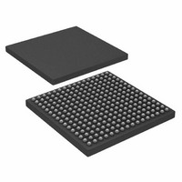
AD6636CBCZ Analog Devices Inc, AD6636CBCZ Datasheet - Page 68

AD6636CBCZ
Manufacturer Part Number
AD6636CBCZ
Description
IC DIGITAL DWNCONV 4CH 256CSPBGA
Manufacturer
Analog Devices Inc
Series
AD6636r
Datasheet
1.AD6636BCPCB.pdf
(80 pages)
Specifications of AD6636CBCZ
Rf Type
Cellular, CDMA2000, EDGE, GPRS, GSM
Number Of Mixers
1
Secondary Attributes
Down Converter
Current - Supply
450mA
Voltage - Supply
3 V ~ 3.6 V
Package / Case
256-CSPBGA
Brief Features
4/6 Independent Wideband Processing Channel, Quadrature Correction & DC Correction For Complex Input
Supply Voltage Range
1.7V To 1.9V
Operating Temperature Range
-40°C To +85°C
Ic Function
Digital Down Converter (DDC)
Rohs Compliant
Yes
Pin Count
256
Screening Level
Industrial
Package Type
CSPBGA
Lead Free Status / RoHS Status
Lead free / RoHS Compliant
Frequency
-
Gain
-
Noise Figure
-
Lead Free Status / Rohs Status
Compliant
Available stocks
Company
Part Number
Manufacturer
Quantity
Price
Company:
Part Number:
AD6636CBCZ
Manufacturer:
ADI
Quantity:
240
AD6636
Port A Power Monitor Period <23:0>
This register is used in the power monitoring logic to set the
period of time for which ADC input data is monitored. This
value represents the monitor period in number of ADC port
clock cycles.
Port A Power Monitor Output <23:0>
This register is read-only and contains the current status of the
power monitoring logic output. The output is dependent on the
power monitoring mode selected. When the power monitor
block is enabled, this register is updated at the end of each
power monitor period. This register is updated even if an
interrupt signal is not generated.
Port A Upper Threshold <9:0>
This register serves the dual purpose of specifying the upper
threshold value in the gain control block and in the power
monitoring block, depending on which block is active. Any
ADC port input data having a magnitude greater than this value
triggers a gain change in the gain control block. Any ADC port
input data having a magnitude greater than this value is
monitored in the power monitoring block (in peak detect or
threshold crossing mode). The value of the register is compared
with the absolute magnitude of the input port data. For real
input, the absolute magnitude is the same as the input data; for
positive and negative data, the absolute magnitude is the value
of the data after removing the negative sign.
Port A Lower Threshold <9:0>
This register is used in the gain control block and represents the
magnitude of the lower threshold for ADC port input data. Any
ADC input data having a magnitude below the lower threshold
initiates the dwell time counter. The value of the register is
compared with the absolute magnitude of the input port data.
For real input, the absolute magnitude is the same as the input
data; for positive and negative data, the absolute magnitude is
the value of the data after removing the negative sign.
Port A Signal Monitor <4:0>
This register controls the functions of the power monitoring
block.
<4>: Disable Power Monitor Period Timer Bit. When this bit is
set, the power monitor period timer no longer controls the
update of the power monitor holding register. A user read to the
power monitor holding register updates this register. When this
bit is cleared, the power monitor period register controls the
timer and, therefore, controls the update rate of the power
monitor holding register.
<3>: Clear-on-Read Bit. When this bit is set, the power monitor
holding register is cleared every time this register is read. This
bit controls whether the power monitoring function is cleared
after a read of the power monitor period register. If this bit is
Rev. A | Page 68 of 80
set, the monitoring function is cleared after the read. If this bit
is Logic 0, the monitoring function is not cleared. This bit is a
don’t care if the disable integration counter bit is clear.
<2:1>: Monitor Function Select Bits. Table 34 lists the functions
of these bits.
Table 34. Monitor Function Select Bits
Monitor Function Select
00
01
10
11
<0>: Monitor Enable Bit. When this bit is set, the power
monitoring function is enabled and operates as selected by
Bits <2:1> of the signal monitor register. When this bit is
cleared, the power monitoring function is disabled and the
signal monitor register <2:1> bits are don’t care. This bit
defaults to 0 on power-up.
Note: Gain control, dwell timer, power monitor period, signal
monitor, power monitoring output, and lower threshold and
upper threshold registers for Port B, Port C, and Port D work
similarly to the corresponding registers definitions for Port A.
CHANNEL REGISTER MAP
Channel control registers are common to all six channels and
access to specific channels is determined by the channel I/O
access register (Address 0x02).
NCO Control <8:0>
These bits control the NCO operation.
<8:7>: NCO Sync Start Select Bits. These bits determine which
SYNC input pin is used by this channel for a start synchroniza-
tion operation. Table 35 describes the selection.
Table 35. Sync Start Select Bits
NCO Control <8:7>
00
01
10
11
<6:5>: NCO Sync Hop Select Bits. These bits determine which
SYNC input pin is used by this channel for a hop synchroniza-
tion operation. Table 36 describes the selection.
Table 36. Sync Hop Select Bits
NCO Control <6:5>
00
01
10
11
<4>: This bit is open.
SYNC Pin Used for Start Synchronization
SYNC0
SYNC1
SYNC2
SYNC3
SYNC Pin Used for Hop Synchronization
SYNC0
SYNC1
SYNC2
SYNC3
Function Enabled
Peak Detect Mode
Mean Power Monitor Mode
Threshold Crossing Mode
Invalid Selection


