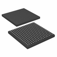
AD6636CBCZ Analog Devices Inc, AD6636CBCZ Datasheet - Page 47

AD6636CBCZ
Manufacturer Part Number
AD6636CBCZ
Description
IC DIGITAL DWNCONV 4CH 256CSPBGA
Manufacturer
Analog Devices Inc
Series
AD6636r
Datasheet
1.AD6636BCPCB.pdf
(80 pages)
Specifications of AD6636CBCZ
Rf Type
Cellular, CDMA2000, EDGE, GPRS, GSM
Number Of Mixers
1
Secondary Attributes
Down Converter
Current - Supply
450mA
Voltage - Supply
3 V ~ 3.6 V
Package / Case
256-CSPBGA
Brief Features
4/6 Independent Wideband Processing Channel, Quadrature Correction & DC Correction For Complex Input
Supply Voltage Range
1.7V To 1.9V
Operating Temperature Range
-40°C To +85°C
Ic Function
Digital Down Converter (DDC)
Rohs Compliant
Yes
Pin Count
256
Screening Level
Industrial
Package Type
CSPBGA
Lead Free Status / RoHS Status
Lead free / RoHS Compliant
Frequency
-
Gain
-
Noise Figure
-
Lead Free Status / Rohs Status
Compliant
Available stocks
Company
Part Number
Manufacturer
Quantity
Price
Company:
Part Number:
AD6636CBCZ
Manufacturer:
ADI
Quantity:
240
In Figure 42, the PxACK is already pulled high and, therefore,
the 8-bit I data and 8-bit Q data are simultaneously output on
the data bus on the next PCLK rising edge after PxREQ is
driven logic high. The PxIQ signal also goes high to indicate
that I/Q data is available on the data bus. When I/Q data is
being output, the channel indicator pins PxCH[2:0] indicate the
data source (AGC number).
Figure 42 is the timing diagram for interleaved I/Q mode with
the AGC gain word disabled. Figure 43 is a similar timing
diagram with the AGC gain word enabled. I and Q data are as
shown in Figure 39. In the PCLK cycle after the I/Q data, the
AGC gain word is output on the data bus, and the PxGAIN
signal is pulled high to indicate that the gain word is available
on the parallel port. During this PCLK cycle, the PxIQ signal is
pulled low to indicate that I/Q data is not available on the data
bus. Therefore, in parallel I/Q mode, a minimum of two PCLK
cycles is required to output one sample of output data on the
parallel port without and with the AGC gain word, respectively.
The order of data output is dependent on when data arrives at
the port, which is a function of total decimation rate, DRCF/
CRCF decimation phase, and start hold-off values. Priority
order from highest to lowest is AGCs 0, 1, 2, 3, 4, and 5 for both
parallel I/Q and interleaved modes of output.
Parallel Port Pin Functions
Table 25 describes the functions of the pins used by the parallel ports.
Table 25. Parallel Port Pin Functions
Mnemonic
PCLK
PAREQ, PBREQ,
PCREQ
PAACK, PBACK,
PCACK
PAIQ, PBIQ,
PCIQ
PAGAIN,
PBGAIN,
PCGAIN
PACH[2:0],
PBCH[2:0],
PCCH[2:0]
PADATA[15:0],
PBDATA[15:0],
PCDATA[15:0]
I/O
I/O
O
I
Function
PCLK can operate as a master or as a slave. This setting is dependent on the 1-bit PCLK master mode bit in the
Parallel Port Control 2 register. As an output (master mode), the maximum frequency is CLK/N, where CLK is
AD6636 clock and N is an integer divisor of 1, 2, 4, or 8. As an input (slave mode), it can be asynchronous or
synchronous relative to the AD6636 CLK. This pin powers up as an input to avoid possible contentions.
Parallel port output pins change on the rising edge of PCLK.
Active high output. Synchronous to PCLK. A logic high on this pin indicates that data is available to be shifted
out of the port. When an acknowledge signal is received, data starts shifting out and this pin remains high until
all pending data has been shifted out.
Active high asynchronous input. Applying a logic low on this pin inhibits parallel port data shifting. Applying
a logic high to this pin when REQ is high causes the parallel port to shift out data according to the programmed
data mode.
ACK is sampled on the rising edge of PCLK. Assuming that REQ is asserted, the latency from the assertion of ACK
to data appearing at the parallel port output is no more than 1.5 PCLK cycles. ACK can be held high continuously;
in this case, when data becomes available, shifting begins 1 PCLK cycle after the assertion of REQ (see Figure 40,
Figure 41, Figure 42, and Figure 43).
High whenever I data is present on the parallel port data bus; otherwise low. In parallel I/Q mode, both I data
and Q data are available at the same time and, therefore, the PxIQ signal is pulled high.
High whenever the AGC gain word is present on the parallel port data bus; otherwise low.
These pins identify data in both of the parallel port modes. The 3-bit value identifies the source of the data
(AGC number) on the parallel port when it is being shifted out.
Parallel output port data bus. Output format is twos complement. In parallel I/Q mode, 8-bit data is present;
in interleaved I/Q mode, 16-bit data is available.
Rev. A | Page 47 of 80
Master/Slave PCLK Modes
The parallel ports can operate in either master or slave mode.
The mode is set via the PCLK master mode bit in the Parallel
Port Control 2 register. The parallel ports power up in slave
mode to avoid possible contentions on the PCLK pin.
In master mode, PCLK is an output derived by dividing
PLL_CLK down by the PCLK divisor. The PCLK divisor can
have a value of 1, 2, 4, or 8, depending on the 2-bit PCLK
divisor word setting in the Parallel Port Control 2 register. The
highest PLCK rate in master mode is 200 MHz. Master mode is
selected by setting the PCLK master mode bit in the Parallel
Port Control 2 register.
In slave mode, external circuitry provides the PCLK signal.
Slave mode PCLK signals can be either synchronous or
asynchronous. The maximum slave mode PCLK frequency is
also 200 MHz.
PCLK
Rate
=
PLL_CLK
PCLK
Divisor
Rate
AD6636


