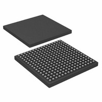
AD6636CBCZ Analog Devices Inc, AD6636CBCZ Datasheet - Page 38

AD6636CBCZ
Manufacturer Part Number
AD6636CBCZ
Description
IC DIGITAL DWNCONV 4CH 256CSPBGA
Manufacturer
Analog Devices Inc
Series
AD6636r
Datasheet
1.AD6636BCPCB.pdf
(80 pages)
Specifications of AD6636CBCZ
Rf Type
Cellular, CDMA2000, EDGE, GPRS, GSM
Number Of Mixers
1
Secondary Attributes
Down Converter
Current - Supply
450mA
Voltage - Supply
3 V ~ 3.6 V
Package / Case
256-CSPBGA
Brief Features
4/6 Independent Wideband Processing Channel, Quadrature Correction & DC Correction For Complex Input
Supply Voltage Range
1.7V To 1.9V
Operating Temperature Range
-40°C To +85°C
Ic Function
Digital Down Converter (DDC)
Rohs Compliant
Yes
Pin Count
256
Screening Level
Industrial
Package Type
CSPBGA
Lead Free Status / RoHS Status
Lead free / RoHS Compliant
Frequency
-
Gain
-
Noise Figure
-
Lead Free Status / Rohs Status
Compliant
Available stocks
Company
Part Number
Manufacturer
Quantity
Price
Company:
Part Number:
AD6636CBCZ
Manufacturer:
ADI
Quantity:
240
AD6636
INTERPOLATING HALF-BAND FILTER
The AD6636 has interpolating half-band FIR filters that
immediately follow the CRCF programmable FIR filters and
precede the second data router. Each interpolating half-band
filter takes 22-bit I and 22-bit Q data from the preceding CRCF
and outputs rounded 22-bit I and 22-bit Q data to the second
data router. A 10-tap fixed-coefficient filter is implemented in
this stage.
The maximum input rate into this block is 17 MHz. Conse-
quently, the maximum output is constrained to 34 MHz. The
normalized coefficients used in the implementation and the
10-bit decimal equivalent value of the coefficients are listed in
Table 22. Other coefficients are 0.
Table 22. Interpolating HB Filter Fixed Coefficients
Coefficient
Number
C1, C11
C3, C9
C5, C7
C6
The half-band filters interpolate the incoming data by 2×. For a
channel running at 2× the chip rate, the half-band can be used
to output channel data at 4× the chip rate. The interpolation
operation creates an image of the baseband signal, which is
filtered out by the half-band filter.
The image rejection of this filter is about 55 dB, but is still
sufficient, because the image is from the desired signal, not an
interfering signal. Note that the interpolating half-band filter
can be enabled by writing a Logic 1 to Bit 9 of the MRCF
control registers.
The frequency response of the interpolating half-band FIR is
shown in Figure 37 with respect to the chip rate. The input rate to
this filter is 2× the chip rate, and the output rate is 4× the chip rate.
–100
–20
–40
–60
–80
0
0
FILTER RESPONSE
Figure 37. Interpolating Half-Band Frequency Response
INTERPOLATING
0.2
HALFBAND
FREQUENCY AS FRACTION OF INPUT RATE
0.4
Normalized
Coefficient
+0.02734375
−0.12890625
+0.603515625
+1
0.6
0.8
0.75
1.0
1.2
1.25
1.4
Decimal Coefficient
(10-Bit)
+14
−66
+309
+512
1.6
1.8
–53
Rev. A | Page 38 of 80
OUTPUT DATA ROUTER
The output data router circuit precedes the six AGCs of the
final output block and immediately follows the interpolating
half-band filters. This block consists of two subblocks. The first
subblock is responsible for combining (interleaving) data from
more than one channel into a single stream of data.
The second subblock can perform two special functions, either
complex filter completion or biphase filtering. The combined
data is passed on to the AGCs.
Interleaving Data
In some cases, filtering using a single channel is insufficient.
For such setups, it is advantageous to combine the filtering
resources of more than one channel.
Multiple channels can be set up to work on the ADC input port
data with the same NCO and filter setups. The decimation
phase values in one of the RCF filters are set such that the
channel filters are exactly out of phase with each other. In the
data router, these multiple channels are interleaved (combined)
to form a single stream of data. Because each individual channel
is decimated more than it would be if a single channel were
filtering, a larger number of filter taps can be calculated.
For example, two channels need to work together to produce a
filter at an output rate of 10 MHz when the input rate is
100 MHz. Each channel is decimated by a factor of 20 (total
decimation) to achieve the desired output rate of 5 MHz each.
This compares to a decimation of 10, if a single channel were
filtering.
The same coefficients are programmed in both channels’ RCF
filters, and the decimation phases are set to 0 and 1. The
decimation phases can be set to 0 for one channel and 1 for the
second channel in the pair. This causes the first channel to
produce the even outputs of the filter, and the second to
produce the odd outputs of the filter. The streams can then be
recombined (interleaved) to produce the desired 10 MHz
output rate. The benefit is that now each channel’s RCF has
time to calculate twice as many taps because it has a lower
output rate.


