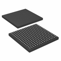
AD6636CBCZ Analog Devices Inc, AD6636CBCZ Datasheet - Page 65

AD6636CBCZ
Manufacturer Part Number
AD6636CBCZ
Description
IC DIGITAL DWNCONV 4CH 256CSPBGA
Manufacturer
Analog Devices Inc
Series
AD6636r
Datasheet
1.AD6636BCPCB.pdf
(80 pages)
Specifications of AD6636CBCZ
Rf Type
Cellular, CDMA2000, EDGE, GPRS, GSM
Number Of Mixers
1
Secondary Attributes
Down Converter
Current - Supply
450mA
Voltage - Supply
3 V ~ 3.6 V
Package / Case
256-CSPBGA
Brief Features
4/6 Independent Wideband Processing Channel, Quadrature Correction & DC Correction For Complex Input
Supply Voltage Range
1.7V To 1.9V
Operating Temperature Range
-40°C To +85°C
Ic Function
Digital Down Converter (DDC)
Rohs Compliant
Yes
Pin Count
256
Screening Level
Industrial
Package Type
CSPBGA
Lead Free Status / RoHS Status
Lead free / RoHS Compliant
Frequency
-
Gain
-
Noise Figure
-
Lead Free Status / Rohs Status
Compliant
Available stocks
Company
Part Number
Manufacturer
Quantity
Price
Company:
Part Number:
AD6636CBCZ
Manufacturer:
ADI
Quantity:
240
<5>: Channel 1 Data Ready Enable Bit. Similar to Bit <9> for
Channel 1.
<4>: Channel 0 Data Ready Enable Bit. Similar to Bit <9> for
Channel 0.
<3>: ADC Port D Power Monitoring Enable Bit. When this bit
is set to Logic 1, the ADC Port D power monitoring interrupt is
enabled allowing an interrupt to be generated when ADC
Port D power monitoring registers are updated. When set to
Logic 1, the ADC Port D power monitoring interrupt is
disabled.
<2>: ADC Port C Power Monitoring Enable Bit. Similar to
Bit <3> for ADC Port C.
<1>: ADC Port B Power Monitoring Enable Bit. Similar to
Bit <3> for ADC Port B.
<0>: ADC Port A Power Monitoring Enable Bit. Similar to
Bit <3> for ADC Port A.
INPUT PORT REGISTER MAP
ADC Input Control Register <27:0>
These bits are general control bits for the ADC input logic.
<27>: PN Active Bit. When this bit is set, the pseudorandom
number generator is active. When this bit is cleared, the PN
generator is disabled and the seed is set to its default value.
<26>: EXP Lock Bit. When this bit is set along with the PN
active bit, then the EXP signal for pseudorandom input is
locked to 000 (giving full-scale input). When this bit is cleared,
EXP bits for pseudorandom input are randomly generated input
data bits.
<25>: Port C Complex Data Active Bit. When this bit is set, the
data inputs on Port C and Port D are interpreted as complex
inputs (Port C for the in-phase signal and Port D for the
quadrature phase signal). This complex input is passed on as
the input from ADC Port C. When this bit is cleared, the data
on ADC Port C and ADC Port D are interpreted as real and
independent input.
Note that complex input mode is available only in CMOS input
mode.
<24>: Port A Complex Data Active Bit. When this bit is set, the
data input on Port A and Port B are interpreted as complex
input (Port A for the in-phase signal and Port B for the
quadrature phase signal). This complex input is passed on as
input from ADC Port A. When this bit is cleared, the data on
ADC Port A and ADC Port B are interpreted as real and
independent input.
Note that complex input mode is available only in CMOS input
mode.
Rev. A | Page 65 of 80
<23>: Channel 5 Complex Data Input Bit. When this bit is set,
Channel 5 gets complex input data from the source that is
selected by the crossbar mux select bits. When this bit is cleared,
Channel 5 receives real input data (see Table 32).
<22:20>: Channel 5 Crossbar Mux Select Bits. These bits select
the source of input data for Channel 5 (see Table 32).
Table 32. Channel 5 Input Configuration
Complex
Data Input
Bit
0
0
0
0
0
1
1
1
<19>: Channel 4 Complex Data Input Bit. Similar to Bit <23>
for Channel 4.
<18:16>: Channel 4 Crossbar Mux Select Bits. Similar to Bits
<22:20> for Channel 4.
<15>: Channel 3 Complex Data Input Bit. Similar to Bit <23>
for Channel 3.
<14:12>: Channel 3 Crossbar Mux Select Bits. Similar to Bits
<22:20> for Channel 3.
<11>: Channel 2 Complex Data Input Bit. Similar to Bit <23>
for Channel 2.
<10:8>: Channel 2 Crossbar Mux Select Bits. Similar to Bits
<22:20> for Channel 2.
<7>: Channel 1 Complex Data Input Bit. Similar to Bit <23> for
Channel 1.
<6:4>: Channel 1 Crossbar Mux Select Bits. Similar to Bits
<22:20> for Channel 1.
<3>: Channel 0 Complex Data Input Bit. Similar to Bit <23> for
Channel 0.
<2:0>: Channel 0 Crossbar Mux Select Bits. Similar to Bits
<22:20> for Channel 0.
ADC CLK Control Register <11:0>
These bits control the ADC clocks and internal PLL clock.
<11>: ADC Port D CLK Invert Bit. When this bit is set, the
inverted ADC Port D clock is used to register ADC Input
Port D data into the part. When this bit is cleared, the clock is
used as is, without any inversion or phase change.
Crossbar
Mux Select
Bits
000
001
010
011
100
000
001
010
Configuration
ADC Port A Drives Input (Real)
ADC Port B Drives Input (Real)
ADC Port C Drives Input (Real)
ADC Port D Drives Input (Real)
PN Sequence Drives Input (Real)
Ports A and B Drive Complex Input
Ports C and D Drive Complex Input
PN Sequence Drives Complex Input
AD6636


