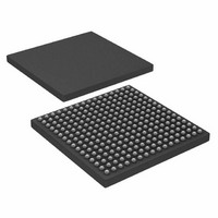
AD6636CBCZ Analog Devices Inc, AD6636CBCZ Datasheet - Page 78

AD6636CBCZ
Manufacturer Part Number
AD6636CBCZ
Description
IC DIGITAL DWNCONV 4CH 256CSPBGA
Manufacturer
Analog Devices Inc
Series
AD6636r
Datasheet
1.AD6636BCPCB.pdf
(80 pages)
Specifications of AD6636CBCZ
Rf Type
Cellular, CDMA2000, EDGE, GPRS, GSM
Number Of Mixers
1
Secondary Attributes
Down Converter
Current - Supply
450mA
Voltage - Supply
3 V ~ 3.6 V
Package / Case
256-CSPBGA
Brief Features
4/6 Independent Wideband Processing Channel, Quadrature Correction & DC Correction For Complex Input
Supply Voltage Range
1.7V To 1.9V
Operating Temperature Range
-40°C To +85°C
Ic Function
Digital Down Converter (DDC)
Rohs Compliant
Yes
Pin Count
256
Screening Level
Industrial
Package Type
CSPBGA
Lead Free Status / RoHS Status
Lead free / RoHS Compliant
Frequency
-
Gain
-
Noise Figure
-
Lead Free Status / Rohs Status
Compliant
Available stocks
Company
Part Number
Manufacturer
Quantity
Price
Company:
Part Number:
AD6636CBCZ
Manufacturer:
ADI
Quantity:
240
AD6636
• The CPUCLK (SCLK) is the clock used for programming via
• CLKA, CLKB, CLKC, and CLKD are used as individual
• The microport data bus is 16 bits wide. Both 8-bit and 16-bit
• The output parallel port has a one clock cycle overhead. If
• The number of clock cycles required for each channel can be
If JTAG is used, the designer should ensure that the TRST pin
is pulled low during power-up. After the power supplies have
settled to nominal values (1.8 V and 3.3 V), the TRST pin can
be pulled high for JTAG control. When JTAG control is no
longer required, the TRST pin should ideally be pulled low
again.
the microport (serial port). This clock needs to be provided
by the designer to the part (slave clock). The designer should
ensure that this clock’s frequency is less than or equal to the
frequency of the CLKA signal. Additionally, the frequency of
the CPUCLK (SCLK) should always be less than 100 MHz.
clocks to input data into Input Port A, Input Port B, Input
Port C, and Input Port D, respectively. These clocks must
have the same frequency and should be generated ideally
from the same clock source. Note that CLKA is used to drive
the internal circuitry and the PLL clock multiplier. Therefore,
even if Input Port A is not used, CLKA should be driven by
the input clock.
modes are available using this part. If 8-bit mode is used, the
MSB of the data bus (D[15:8]) can be left floating or
connected to GND.
two channels (with the same data rates) are output on one
output port in 16-bit interleaved I/Q mode along with an
AGC word, this requires three clock cycles for one sample
from each channel (one clock each for I data, Q data, and
gain data). Therefore, the total number of clock cycles
required to output the data is 3 clocks/channel × 2 channels +
1 (overhead) = 7 clock cycles.
3 (interleaved I + Q + gain word), 2 (parallel I /Q + gain), 2
(interleaved I + Q), or 1 (interleaved I/Q). Designers should
make sure that sufficient time is allowed to output these
channels on one output port. Also note that the I, Q, and gain
Rev. A | Page 78 of 80
• When CRCF and DRCF filters are disabled, the coefficient
• In the Intel mode microport, the beginning of a read and
• In both Intel and Motorola microport modes care should be
• In both Intel and Motorola modes, if CS is held low even after
• In SPI mode programming, the SCS pin needs to go high
for a particular channel all come out on a single output port
and cannot be divided among output ports.
memory cannot be read back because the clock to the
coefficient RAM is also off.
write access is indicated by the RDY pin going low. The
access is complete only when the RDY pin goes high. In the
Motorola mode microport, the completion of a read and
write access is indicated by the DTACK going low. In both
modes, CS , RD ( DS ), and WR (R/ W ) should be active until
access is complete; otherwise, an incomplete access results.
taken not to read or write, to or from, addresses beyond those
defined by the memory map (Address 0xE8 to
Address 0xFF). Attempting to access these addresses causes
the bus to hang because DTACK (RDY) does not go high to
signal the end of the access.
microport read or write access is complete, the microport
initiates a second access. This is a problem while writing or
reading from coefficient RAM, where each access writes to or
reads from a different RAM address. This can be corrected by
writing to one coefficient RAM address at a time, that is, the
coefficient start and stop address registers have the same
value.
(inactive) after writing or reading each byte (eight clock
cycles on the SCLK pin).


