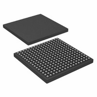
AD6636CBCZ Analog Devices Inc, AD6636CBCZ Datasheet - Page 23

AD6636CBCZ
Manufacturer Part Number
AD6636CBCZ
Description
IC DIGITAL DWNCONV 4CH 256CSPBGA
Manufacturer
Analog Devices Inc
Series
AD6636r
Datasheet
1.AD6636BCPCB.pdf
(80 pages)
Specifications of AD6636CBCZ
Rf Type
Cellular, CDMA2000, EDGE, GPRS, GSM
Number Of Mixers
1
Secondary Attributes
Down Converter
Current - Supply
450mA
Voltage - Supply
3 V ~ 3.6 V
Package / Case
256-CSPBGA
Brief Features
4/6 Independent Wideband Processing Channel, Quadrature Correction & DC Correction For Complex Input
Supply Voltage Range
1.7V To 1.9V
Operating Temperature Range
-40°C To +85°C
Ic Function
Digital Down Converter (DDC)
Rohs Compliant
Yes
Pin Count
256
Screening Level
Industrial
Package Type
CSPBGA
Lead Free Status / RoHS Status
Lead free / RoHS Compliant
Frequency
-
Gain
-
Noise Figure
-
Lead Free Status / Rohs Status
Compliant
Available stocks
Company
Part Number
Manufacturer
Quantity
Price
Company:
Part Number:
AD6636CBCZ
Manufacturer:
ADI
Quantity:
240
MEMORY
MEMORY
gives the delay in input clock cycles. A programmable pipeline
delay given by the 6-bit value (maximum delay of 63 clock
cycles) is placed between the gain control output and the
EXP[2:0] input. Therefore, the external gain-ranging block’s
settling delays are compensated for in the AD6636.
Note that any gain changes that are initiated during the
relinearization period are ignored. For example, if the AD6636
detects that a gain adjustment is required during the relineariza-
tion period of a previous gain adjustment, then the new
adjustment is ignored.
Setting Up the Gain Control Block
To set up the gain control block for individual input ports, the
individual upper threshold registers and lower threshold
registers should be written with appropriate values. The 10-bit
values written into upper and lower threshold registers are
compared to the 10 MSB bits of the absolute magnitude
calculated using the input port data. The 20-bit dwell timer
register should have the appropriate number of clock cycles to
provide temporal hysteresis.
A 6-bit relinearization pipeline delay word is set to synchronize
with the settling delay in the external gain ranging circuitry.
Finally, the gain control enable bit is written with Logic 1 to
activate the gain control block. On enabling, the gain control
output bits are made 000 (output on EXP[2:0] pins), which
represent the minimum gain for the external gain-ranging
circuitry and corresponding minimum attenuation during
relinearization. The normal functioning takes over, as explained
previously in this section.
Complex Inputs
For complex inputs (formed by pairing two input ports), only
one set of EXP[2:0] pins should be used as the gain control
output. For the pair of Input Port A and Input Port B, gain
control circuitry for Input Port A is active, and EXPA[2:0]
should be connected externally as the gain control output. The
gain control circuitry for Input Port B is not activated (shut
down), and EXPB[2:0] is forced to be equal to EXP[2:0].
FROM INPUT
FROM
FROM
MAP
MAP
PORTS
THRESHOLD
THRESHOLD
REGISTER
REGISTER
LOWER
UPPER
Figure 25. AD6636 Gain Control Block Diagram
B
A
A
B
COMPARE
COMPARE
A > B
A < B
EXTERNAL GAIN
EXTERNAL GAIN
DECREASE
INCREASE
DWELL
TIMER
DEC
INC
EXP GEN
EXP [2:0]
Rev. A | Page 23 of 80
ADC INPUT PORT MONITOR FUNCTION
The AD6636 provides a power-monitor function that can
monitor and gather statistics about the received signal in a
signal chain. Each input port is equipped with an individual
power-monitor function that can operate both in real and
complex modes of the input port. This function block can
operate in one of three modes, which measure the following
over a programmable period of time:
•
•
•
These functions are controlled via the 2-bit power-monitor
function select bits of the power monitor control register for
each individual input port. The input ports can be set for
different modes, but only one function can be active at a time
for any given input port.
The three modes of operation can function continuously over a
programmable time period. This time period is programmed as
the number of input clock cycles in a 24-bit ADC monitor
period register (AMPR). This register is separate for each input
port. An internal magnitude storage register (MSR) is used to
monitor, accumulate, or count, depending on the mode of
operation.
Peak Detector Mode (Control Bits 00)
The magnitude of the input port signal is monitored over a
programmable time period (given by AMPR) to give the peak
value detected. This mode is set by programming Logic 0 in the
power-monitor function select bits of the power-monitor
control register for each individual input port. The 24-bit
AMPR must be programmed before activating this mode.
After enabling this mode, the value in the AMPR is loaded into
a monitor period timer and the countdown is started. The
magnitude of the input signal is compared to the MSR, and the
greater of the two is updated back into the MSR. The initial
value of the MSR is set to the current ADC input signal
magnitude. This comparison continues until the monitor
period timer reaches a count of 1.
When the monitor period timer reaches a count of 1, the value
in the MSR is transferred to the power-monitor holding register,
which can be read through the microport or the serial port. The
monitor period timer is reloaded with the value in the AMPR,
and the countdown is started. Also, the first input sample’s
magnitude is updated in the MSR, and the comparison and
update procedure, as explained above, continues. If the
interrupt is enabled, an interrupt is generated, and the interrupt
status register is updated when the AMPR reaches a count of 1.
Peak power
Mean power
Number of samples crossing a threshold
AD6636


